Pin description – Rainbow Electronics MAX6934 User Manual
Page 6
MAX6922/MAX6932/MAX6933/MAX6934
27-, 28-, and 32-Output, 76V,
Serial-Interfaced VFD Tube Drivers
6
_______________________________________________________________________________________
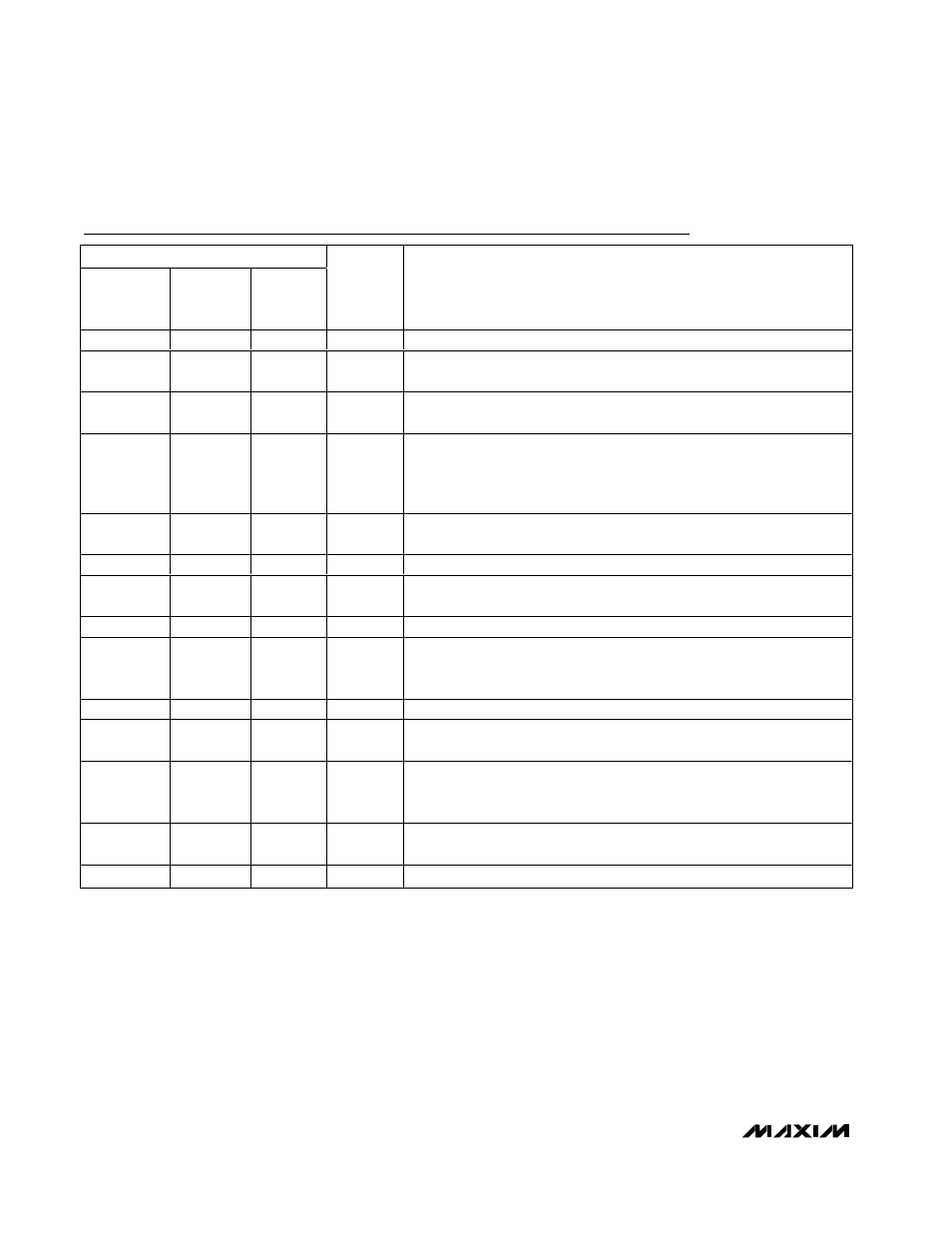
PIN
MAX6922/
MAX6934
PLCC
MAX6932/
MAX6933
SSOP
MAX6934
THIN QFN
NAME
FUNCTION
1
1
39
V
BB
VFD Supply Voltage
2
2
40
DOUT
(MAX6932)
Serial-Data Output. Data is clocked out of the internal shift register to DOUT
on CLK’s falling edge. For the MAX6933 only—VFD anode and grid driver.
2
(OUT27)
(MAX6933)
(OUT27 is a push-pull output swinging from V
BB
to V
SS
.)
3, 4, 5, 7–
17, 19, 20,
25, 26, 27,
30–42
—
1–11, 13,
14, 19, 20,
21, 24–36,
41, 42, 43
OUT0 to
OUT31
VFD Anode and Grid Drivers. OUT_ are push-pull outputs swinging from
GND to V
SS
for the MAX6922 and from V
BB
to V
SS
for the MAX6934.
—
3 –13, 15,
16, 21–34
—
OUT0 to
OUT26
VFD Anode and Grid Drivers. OUT_ are push-pull outputs swinging from
V
BB
to V
SS
.
6, 28, 29
—
22, 23, 44
N.C.
No Connection. Not internally connected.
18
—
—
N.C. (V
SS
)
For the MAX6922—No Connection. Not internally connected. For the
MAX6934—bias supply voltage.
—
14
12
V
SS
Bias Supply Voltage
21
17
15
BLANK
Blanking Input. High forces outputs OUT_ low without altering the contents
of the output latches. Low enables outputs OUT_ to follow the state of the
output latches.
22
18
16
GND
Ground
23
19
17
CLK
Serial-Clock Input. Data is loaded into the internal shift register on CLK’s
rising edge. On CLK’s falling edge, data is clocked out of DOUT.
24
20
18
LOAD
Load Input. Data is loaded transparently from the internal shift register to the
output latch while LOAD is high. Data is latched into the output latch on
LOAD's rising edge, and retained while LOAD is low.
43
35
37
DIN
Serial-Data Input. Data is loaded into the internal shift register on CLK’s
rising edge.
44
36
38
V
CC
Logic Supply Voltage
Pin Description