Pin description, Typical operating characteristics (continued) – Rainbow Electronics MAX15022 User Manual
Page 8
MAX15022
Dual, 4A/2A, 4MHz, Step-Down DC-DC
Regulator with Dual LDO Controllers
8
_______________________________________________________________________________________
Pin Description
PIN
NAME
FUNCTION
1
SEL
Track/Sequence Select Input. Connect SEL to SGND to configure the device as a sequencer. Connect
SEL to AVIN for tracking with output 1 as the master. Leave SEL unconnected for tracking with output 2
as the master. Use the output with the higher voltage as the master and the output with the lower voltage
as the slave.
2, 7, 8
PGND1
Power Ground Connection for Regulator 1. Connect the negative terminals of the input and output filter
capacitors to PGND1. Connect PGND1 externally to SGND at a single point, typically at the negative
terminal of the input bypass capacitor.
3, 6
LX1
Inductor Connection for Regulator 1. LX1 is the drain connection of the internal high-side p-channel
MOSFET and the drain connection of the internal synchronous n-channel MOSFET for regulator 1.
4, 5
PVIN1
Input Supply Voltage for Regulator 1. Connect PVIN1 to an external voltage source from 2.5V to 5.5V.
Bypass PVIN1 to PGND1 with a 1μF (min) ceramic capacitor.
9
DVDD1
Switch Driver Supply for Regulator 1. Connect externally to PVIN1.
10
EN1
Enable Input for Regulator 1. When configured as a sequencer, EN1 must exceed 1.225V (typ) for the
PWM controller to begin regulating output 1. When configured as a tracker, connect EN1 to the center
tap of a resistive divider from the regulator 2 output.
11
FB1
Feedback Regulation Point for Regulator 1. Connect FB1 to the center tap of a resistive divider from the
regulator 1 output to SGND to set the output voltage. The FB1 voltage regulates to 0.6V (typ).
12
COMP1
Error-Amplifier Output for Regulator 1. Connect COMP1 to the compensation feedback network.
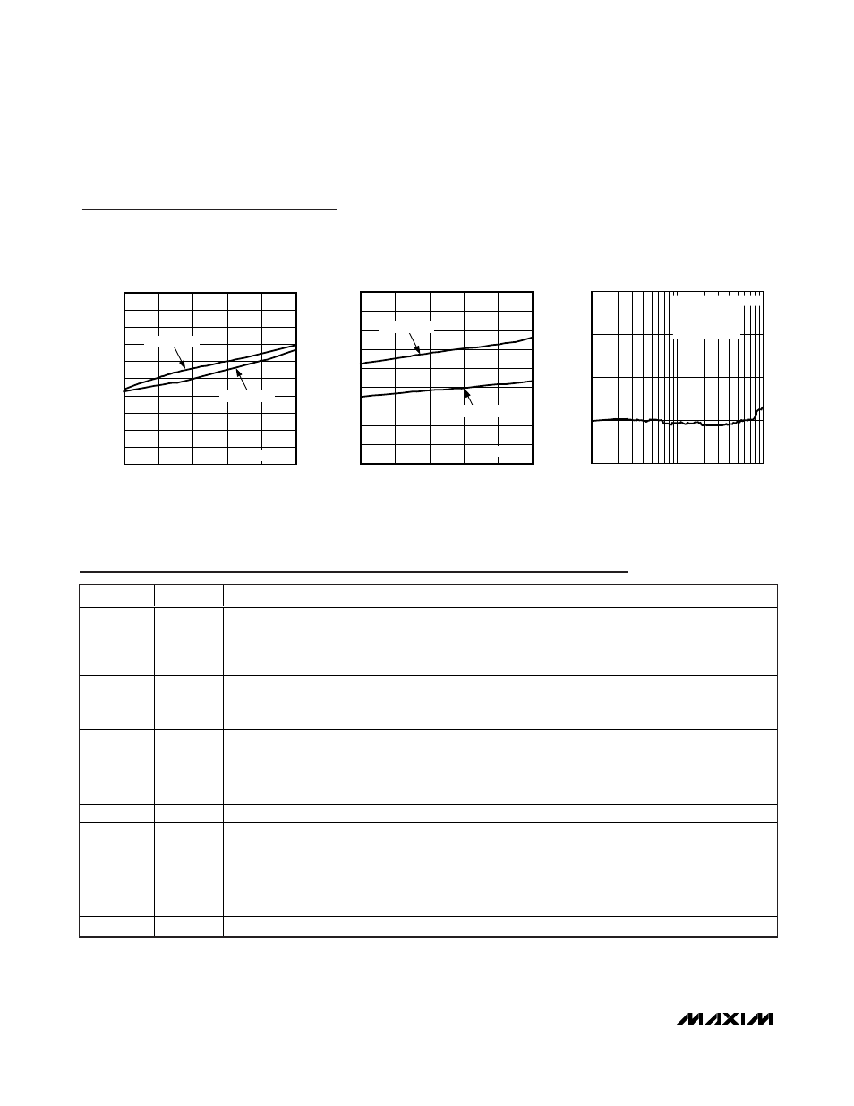
CHANNEL 3 OUTPUT VOLTAGE
vs. INPUT VOLTAGE
MAX15022 toc21
SUPPLY VOLTAGE (V)
OUTPUT VOLTAGE (V)
4.98
4.46
3.94
3.42
2.455
2.460
2.465
2.470
2.475
2.480
2.485
2.490
2.495
2.500
2.450
2.90
5.50
I
OUT3
= 500mA
I
OUT3
= 10mA
V
OUT3
= 2.5V
CHANNEL 4 OUTPUT VOLTAGE
vs. INPUT VOLTAGE
MAX15022 toc22
SUPPLY VOLTAGE (V)
OUTPUT VOLTAGE (V)
4.98
4.46
3.94
3.42
1.175
1.180
1.185
1.190
1.195
1.200
1.205
1.210
1.215
1.170
2.90
5.50
I
OUT4
= 10mA
I
OUT4
= 500mA
V
OUT4
= 1.5V
LDO POWER-SUPPLY REJECTION RATIO
MAX15022 toc23
FREQUENCY (Hz)
PSRR (dB)
100
-70
-60
-50
-40
-30
-20
-10
0
-80
10
1000
V
IN
= 3.3V, V
OUT3
= 2.5V,
I
OUT3
= 10mA,
100mV
P-P
SIGNAL
APPLIED TO V
IN
Typical Operating Characteristics (continued)
(V
AVIN
= V
DVDD1
= V
DVDD2
= V
PVIN1
= V
PVIN2
= 5V, V
OUT1
= 3.3V, V
OUT2
= 1.5V, V
PGND_
= 0V, R
T
= 16.5k
Ω. T
A
= +25°C, unless
otherwise noted.)