Rainbow Electronics MAX15022 User Manual
Page 19

MAX15022
Dual, 4A/2A, 4MHz, Step-Down DC-DC
Regulator with Dual LDO Controllers
______________________________________________________________________________________
19
Type II: Compensation when f
CO
> f
ZERO, ESR
When the f
CO
is greater than f
ESR
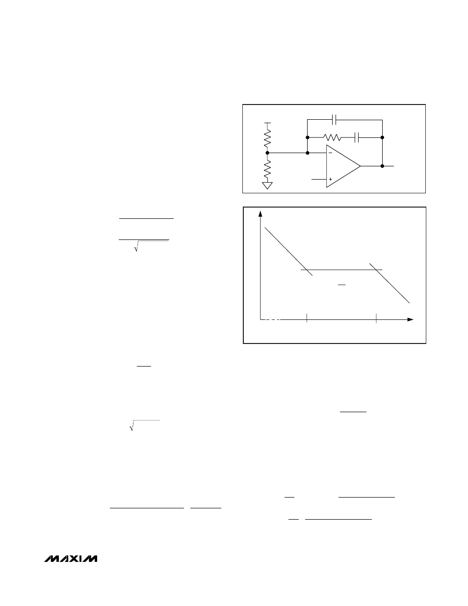
, a Type II compensa-
tion network provides the necessary closed-loop com-
pensated response. The Type II compensation network
provides a midband compensating zero and a high-fre-
quency pole (see Figures 5a and 5b).
R
F
C
F
provides the midband zero f
MID,ZERO
, and
R
F
C
CF
provides the high-frequency pole, f
HIGH,POLE
.
Use the following procedure to calculate the compen-
sation network components.
Calculate the f
ESR
and LC double pole, f
LC
:
where C
OUT
is the regulator output capacitor and ESR
is the series resistance of C
OUT
. See the
Output-
Capacitor Selection
section for more information on cal-
culating C
OUT
and ESR.
Set the compensator’s leading zero, f
Z1
, at or below the
filter’s resonant double-pole frequency from:
Set the compensator’s high-frequency pole, f
P1
, at or
below one-half the switching frequency, f
SW
:
To maximize the compensator’s phase lead, set the
desired crossover frequency, f
CO
, equal to the geomet-
ric mean of the compensator’s leading zero, f
Z1
, and
high-frequency pole, f
P1
, as follows:
Select the feedback resistor, R
F
, in the range of 3.3k
Ω
to 30k
Ω.
Calculate the gain of the modulator (Gain
MOD
)—com-
prised of the regulator’s PWM, LC filter, feedback divider,
and associated circuitry—at the desired crossover fre-
quency, f
CO
, using the following equation:
where V
FB
is the 0.6V (typ) FB_ input-voltage set-point,
L is the value of the regulator inductor, ESR is the
series resistance of the output capacitor, and V
OUT_
is
the desired output voltage.
The gain of the error amplifier (Gain
E/A
) in the midband
frequencies is:
The total loop gain is the product of the modulator gain
and the error amplifier gain at f
CO
and should be set
equal to 1 as follows:
Gain
MOD
x Gain
E/A
= 1
So:
20 log
20 log
0dB
R
R
4 ESR x V
2
f
L x V
1
10
R
R
10
4 ESR x V
2
f
L x V
F
1
FB
CO
OUT_
F
1
FB
CO
OUT_
Ч
+
Ч
=
Ч
Ч
Ч
Ч
=
⎡
⎣
⎢
⎤
⎦
⎥
Ч
Ч
Ч
⎡
⎣
⎢
⎢
⎤
⎦
⎥
⎥
π
π
Gain
R [k ]
R [k ]
E/A
F
1
=
Ω
Ω
Gain
4(V/V)
ESR [m ]
2
f
[kHz] L[ H]
V
[V]
V
[V]
MOD
CO
FB
OUT_
=
Ч
Ч
Ч
(
)
Ч
Ω
π
μ
f
f
f
CO
Z1
P1
=
×
f
f
2
P1
SW
≤
f
f
Z1
LC
≤
f
1
2
ESR C
f
1
2
L C
ESR
OUT
LC
OUT
=
Ч
Ч
≈
Ч
Ч
π
π
R
1
V
REF
R
F
FB_
COMP_
V
OUT_
R
2
C
F
C
CF
Figure 5a. Type II Compensation Network
GAIN
(dB)
1ST ASYMPTOTE
(
ωR
1
C
F
)
-1
2ND ASYMPTOTE
R
F
R
I
3RD ASYMPTOTE
(
ωR
F
C
CF
)
-1
ω (rad/sec)
1ST POLE
(AT ORIGIN)
2ND POLE
(R
F
C
CF
)
-1
1ST ZERO
(R
F
C
F
)
-1
( )
-1
Figure 5b. Type II Compensation Network Response
