Rainbow Electronics MAX15022 User Manual
Page 18

MAX15022
Dual, 4A/2A, 4MHz, Step-Down DC-DC
Regulator with Dual LDO Controllers
18
______________________________________________________________________________________
As seen in Figure 4b, a Type II compensator provides for
stable closed-loop operation, leveraging the +20dB/
decade slope of the capacitor’s ESR zero, while extend-
ing the closed-loop gain bandwidth of the regulator. The
zero crossover now occurs at approximately three times
the uncompensated crossover frequency, f
CO
.
The Type II compensator’s midfrequency gain (approxi-
mately 12dB shown here) is designed to compensate
for the power modulator’s attenuation at the desired
crossover frequency, f
CO
(Gain
E/A
+ Gain
MOD
= 0dB at
f
CO
). In this example, the power modulator’s inherent
-20dB/decade rolloff above the ESR zero (f
ZERO, ESR
)
is leveraged to extend the active regulation gain band-
width of the voltage regulator. As shown in Figure 4b,
the net result is a three times increase in the regulator’s
gain bandwidth while providing greater than 75° of
phase margin (the difference between Gain
E/A
and
Gain
MOD
respective phases at crossover, f
CO
).
Other filter schemes pose their own problems. For
instance, when choosing high-quality filter capacitor(s),
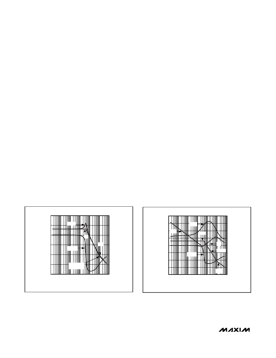
e.g. MLCCs, the inherent ESR zero may occur at a
much higher frequency, as shown in Figure 4c.
As with the previous example, the actual gain and
phase response is overlaid on the power modulator’s
asymptotic gain response. One readily observes the
more dramatic gain and phase transition at or near the
power modulator’s resonant frequency, f
LC
, versus the
gentler response of the previous example. This is due
to the filter components’ lower parasitic (DCR and ESR)
and corresponding higher frequency of the inherent
ESR zero. In this example, the desired crossover fre-
quency occurs below the ESR zero frequency.
In this example, a compensator with an inherent midfre-
quency double-zero response is required to mitigate
the effects of the filter’s double-pole phase lag. This is
available with the Type III topology.
As demonstrated in Figure 4d, the Type III’s midfre-
quency double-zero gain (exhibiting a +20dB/decade
slope, noting the compensator’s pole at the origin) is
designed to compensate for the power modulator’s
double-pole -40dB/decade attenuation at the desired
crossover frequency, f
CO
(again, Gain
E/A
+ Gain
MOD
=
0dB at f
CO
) (see Figure 4d).
In the above example, the power modulator’s inherent
(midfrequency) -40dB/decade rolloff is mitigated by the
midfrequency double zero’s +20dB/decade gain to
extend the active regulation gain bandwidth of the volt-
age regulator. As shown in Figure 4d, the net result is
an approximate doubling in the controller’s gain band-
width while providing greater than 55° of phase margin
(the difference between Gain
E/A
and Gain
MOD
respec-
tive phases at crossover, f
CO
).
Design procedures for both Type II and Type III com-
pensators are shown below.
MAGNITUDE (dB)
PHASE (DEGREES)
FREQUENCY (Hz)
-60
-40
-20
0
20
40
-80
-135
-90
-45
0
45
90
-180
MAX15022 fig04c
100
1k
10k
100k
1M
10M
10
|G
MOD
|
|G
MOD
|
ASYMPTOTE
f
LC
f
ESR
< G
MOD
Figure 4c. Power Modulator Gain and Phase Response with
Low-Parasitic Capacitor(s) (MLCCs)
MAX15022 fig04d
MAGNITUDE (dB)
PHASE (DEGREES)
FREQUENCY (Hz)
-60
-40
-20
0
20
40
60
80
-80
-203
-135
-68
0
68
135
203
270
-270
100
1k
10k
100k
1M
10M
10
< G
EA
|G
EA
|
|G
MOD
|
f
LC
f
ESR
f
CO
< G
MOD
Figure 4d. Power Modulator and Type III Compensator Gain
and Phase Response with Low Parasitic Capacitors (MLCCs)
