Rainbow Electronics MAX15022 User Manual
Page 17
MAX15022
Dual, 4A/2A, 4MHz, Step-Down DC-DC
Regulator with Dual LDO Controllers
______________________________________________________________________________________
17
Below are equations that define the power modulator:
R
OUT
is the load resistance of the regulator, f
LC
is the
resonant break frequency of the filter, and f
ESR
is the
ESR zero of the output capacitor. See the
Closed-Loop
Response and Compensation of Voltage-Mode
Regulators
for more information on f
LC
and f
ESR
.
The switching frequency (f
SW
) is programmable
between 500kHz and 4MHz. Typically, the crossover
frequency (f
CO
)—the frequency at which the system’s
closed-loop gain is equal to unity (crosses 0dB)—
should be set at or below one-tenth the switching fre-
quency (f
SW
/10) for stable closed-loop response.
The MAX15022 provides an internal voltage-mode error
amplifier with its inverting input and its output available to
the user for external frequency compensation. The flexi-
bility of external compensation for each controller offers
a wide selection of output filtering components, especial-
ly the output capacitor. For cost-sensitive applications,
use aluminum electrolytic capacitors while for space-
sensitive applications, use low-ESR tantalum or multilay-
er ceramic chip (MLCC) capacitors at the output. The
higher switching frequencies of the MAX15022 allow the
use of MLCC as the primary filter capacitor(s).
First, select the passive and active power components
that meet the application output ripple, component
size, and component cost requirements. Second,
choose the small-signal compensation components to
achieve the desired closed-loop frequency response
and phase margin as outlined below.
Closed-Loop Response and Compensation
of Voltage-Mode Regulators
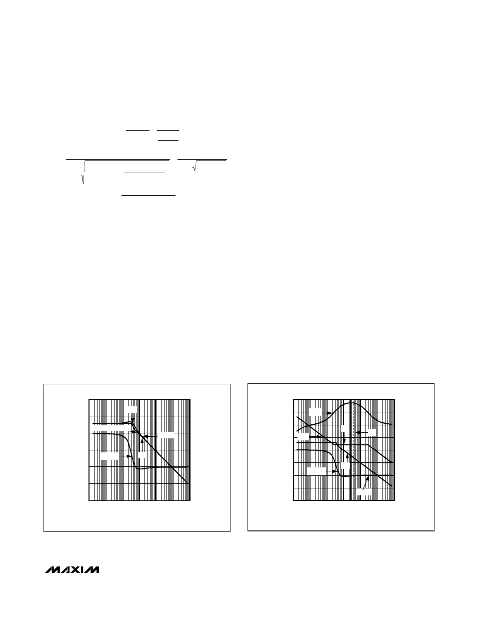
The power modulator’s LC lowpass filter exhibits a vari-
ety of responses, dependent on the value of the L and
C and their parasitics. Higher resistive parasitics
reduce the Q of the circuit, reducing the peak gain and
phase of the system; however, efficiency is also
reduced under these circumstances.
One such response is shown in Figure 4a. In this exam-
ple, the ESR zero occurs relatively close to the filter’s
resonant break frequency, f
LC
. As a result, the power
modulator’s uncompensated crossover is approximate-
ly one third the desired crossover frequency, f
CO
. Note
also, the uncompensated rolloff through the 0dB plane
follows a single-pole, -20dB/decade slope and 90° of
phase lag. In this instance, the inherent phase margin
ensures a stable system; however, the gain-bandwidth
product is not optimized.
Gain
V
V
V
V
4
4V/V
f
1
2
L C
R
ESR
R
DCR
1
2
L C
f
1
2
ESR C
MOD(DC)
AVIN
RAMP
AVIN
AVIN
LC
OUT
OUT
OUT
OUT
ESR
OUT
=
=
=
=
Ч
Ч
Ч
+
+
⎛
⎝⎜
⎞
⎠⎟
≈
Ч
Ч
=
Ч
Ч
π
π
π
MAX15022 fig04a
MAGNITUDE (dB)
PHASE (DEGREES)
-60
-40
-20
0
20
40
-80
100
1k
10k
FREQUENCY (Hz)
100k
1M
10M
10
-135
-90
-45
0
45
90
-180
|G
MOD
|
f
LC
f
ESR
< G
MOD
|G
MOD
| ASYMPTOTE
Figure 4a. Power Modulator Gain and Phase Response with
Lossy Bulk Output Capacitor(s) (Aluminum)
MAX15022 fig04b
MAGNITUDE (dB)
PHASE (DEGREES)
FREQUENCY (Hz)
-60
-40
-20
0
20
40
60
80
-80
-135
-90
-45
0
45
90
135
180
-180
100
1k
10k
100k
1M
10M
10
EA |G EA | |G MOD | f LC f ESR f CO < G MOD Figure 4b. Power Modulator and Type II Compensator Gain and
Phase Response with Lossy Bulk Output Capacitor(s) (Aluminum)