Rainbow Electronics MAX15022 User Manual
Page 20
MAX15022
Dual, 4A/2A, 4MHz, Step-Down DC-DC
Regulator with Dual LDO Controllers
20
______________________________________________________________________________________
Solving for R1:
where V
FB
is the 0.6V (typ) FB_ input-voltage set-point,
L is the value of the regulator inductor, ESR is the
series resistance of the output capacitor, and V
OUT_
is
the desired output voltage.
1) C
F
is determined from the compensator’s leading
zero, f
Z1
, and R
F
as follows:
2) C
CF
is determined from the compensator’s high-fre-
quency pole, f
P1
, and R
F
as follows:
3) Calculate R
2
using the following equation:
where V
FB
= 0.6V (typ) and V
OUT_
is the output voltage
of the regulator.
Type III: Compensation when f
CO
< f
ESR
As indicated above, the position of the output capaci-
tor’s inherent ESR zero is critical in designing an appro-
priate compensation network. When low-ESR ceramic
output capacitors (MLCCs) are used, the ESR zero fre-
quency (f
ESR
) is usually much higher than the desired
crossover frequency (f
CO
). In this case, a Type III com-
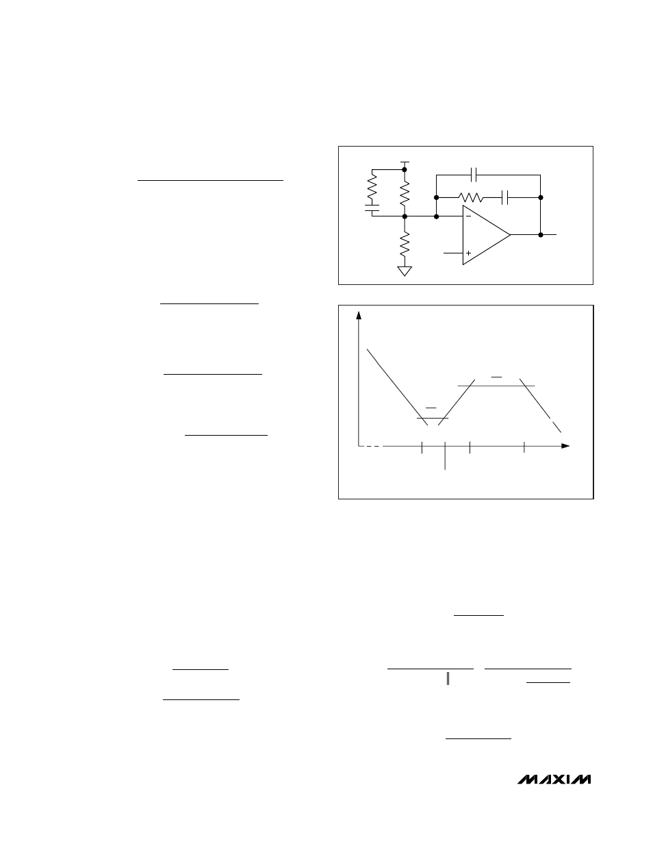
pensation network is recommended (see Figure 6a).
As shown in Figure 6b, the Type III compensation net-
work introduces two zeros and three poles into the con-
trol loop. The error amplifier has a low-frequency pole
at the origin, two zeros, and two higher frequency poles
at the following frequencies:
Two midband zeros (f
Z1
and f
Z2
) are designed to com-
pensate for the pair of complex poles introduced by the
LC filter.
f
P1
introduces a pole at zero frequency (integrator) for
nulling DC output-voltage errors.
f
P1
= at the origin (0Hz)
Depending on the location of the ESR zero (f
ESR
), f
P2
can be used to cancel it, or to provide additional atten-
uation of the high-frequency output ripple.
f
P3
attenuates the high-frequency output ripple.
Since C
CF
<< C
F
then:
f
1
2 R
C
P3
F
CF
=
Ч
Ч
π
f
1
2
R
C C
1
2
R
C
C
C
C
P3
F
F
CF
F
F
CF
F
CF
=
Ч
Ч
(
)
=
Ч
Ч
Ч
+
π
π
f
1
2
R
C
P2
I
I
=
Ч Ч
π
f
1
2
R
C
f
1
2
C
(R
R )
Z1
F
F
Z2
I
1
I
=
Ч
Ч
=
Ч Ч
+
π
π
R [k ] R [k ]
V
[V]
V
[V] V
[V]
2
1
FB
OUT_
FB
Ω
Ω
=
×
−
C
F]
1
2
R [k ] f
[kHz]
CF
F
P1
[
μ
π
=
Ч
Ч
Ω
C [ F]
1
2
R [k ] f
[kHz]
F
F
Z1
μ
π
=
Ч
Ч
Ω
R [k ]
R [k ] 4 ESR[m ] V
[V]
2
f
[kHz] L[ H] V
[V]
1
F
FB
CO
OUT_
Ω
Ω
Ω
=
Ч Ч
Ч
Ч
Ч
Ч
π
μ
R
1
V
REF
R
F
FB_
COMP_
V
OUT_
R
2
C
F
C
CF
R
I
C
I
Figure 6a. Type III Compensation Network
GAIN
(dB)
1ST ASYMPTOTE
(
ωR
I
C
F
)
-1
3RD ASYMPTOTE
(
ωR
F
C
I
)
-1
5TH ASYMPTOTE
(R
I
C
CF
)
-1
ω (rad/sec)
1ST POLE
(AT ORIGIN)
2ND POLE
(R
I
C
I
)
-1
2ND ZERO
(R
1
C
I
)
-1
3RD POLE
(R
F
C
CF
)
-1
1ST ZERO
(R
F
C
F
)
-1
4TH ASYMPTOTE
R
F
R
I
( )
2ND ASYMPTOTE
R
F
R
1
( )
-1
Figure 6b. Type III Compensation Network Response