Rainbow Electronics MAX5974D User Manual
Page 17
MAX5974A/MAX5974B/MAX5974C/MAX5974D
Active-Clamped, Spread-Spectrum,
Current-Mode PWM Controllers
17
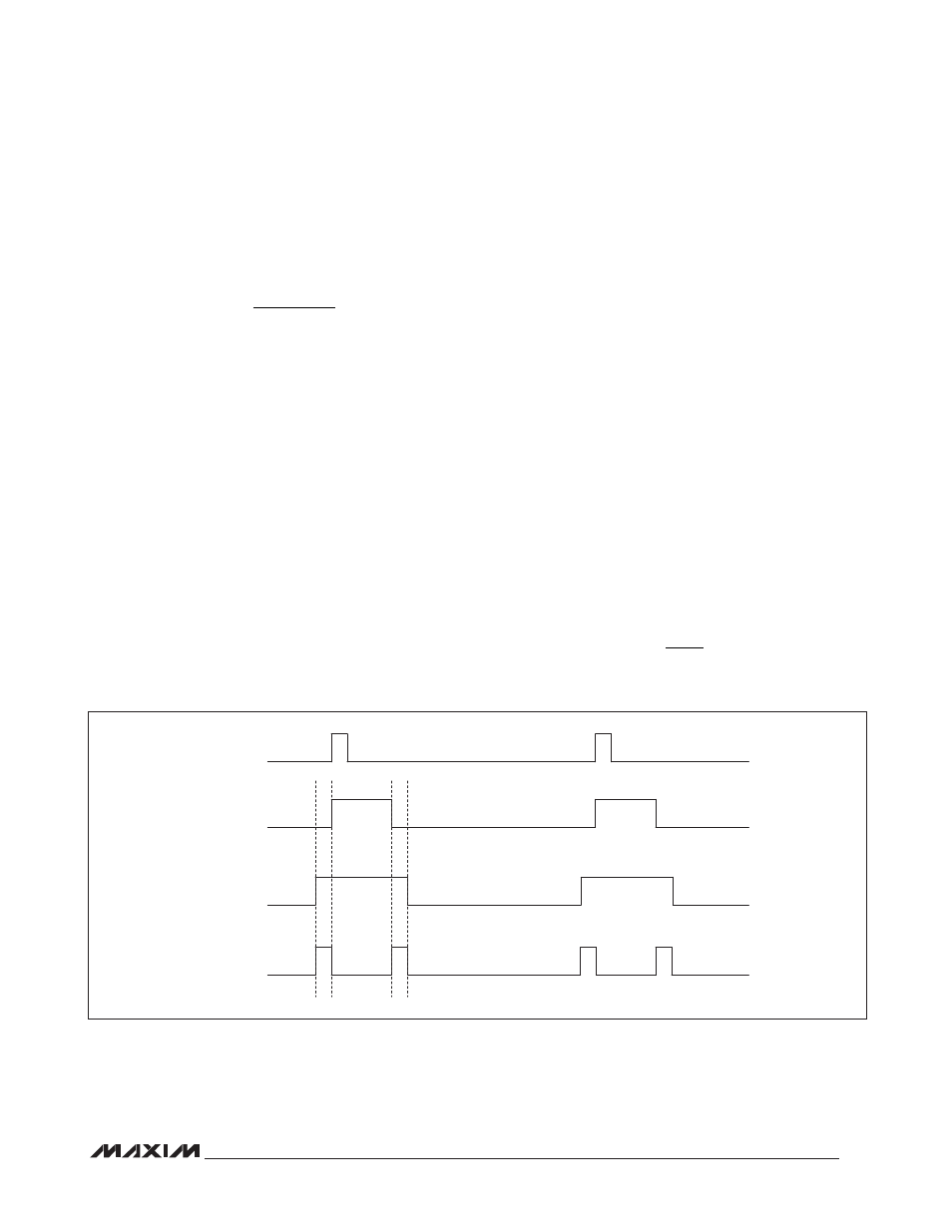
Figure 3. Dead Time Between AUXDRV and NDRV
startup to provide a slow and smooth increase of the
duty cycle to its steady-state value. Calculate the value
of C
SS
as follows:
SS-CH
SS
SS
I
t
C
2V
×
=
where I
SS-CH
(10FA typ) is the current charging C
SS
dur-
ing soft-start and t
SS
is the programmed soft-start time.
A resistor can also be added from the SS pin to GND to
clamp V
SS
< 2V and, hence, program the maximum duty
cycle to be less than 80% (see the Duty-Cycle Clamping
section).
n-Channel MOSFET Gate Driver
The NDRV output drives an external n-channel MOSFET.
NDRV can source/sink in excess of 650mA/1000mA
peak current; therefore, select a MOSFET that yields
acceptable conduction and switching losses. The exter-
nal MOSFET used must be able to withstand the maxi-
mum clamp voltage.
p-Channel MOSFET Gate Driver
The AUXDRV output drives an external p-channel
MOSFET with the aid of a level shifter. The level shifter
consists of C
AUX
, R
AUX
, and D5 as shown in the Typical
Application Circuits. When AUXDRV is high, C
AUX
is
recharged through D5. When AUXDRV is low, the gate
of the p-channel MOSFET is pulled below the source by
the voltage stored on C
AUX
, turning on the pFET.
Add a zener diode between gate to source of the exter-
nal n-channel and p-channel MOSFETs after the gate
resistors to protect V
GS
from rising above its absolute
maximum rating during transient condition (see the
Typical Application Circuits).
Dead Time
Dead time between the main and AUX output edges
allow ZVS to occur, minimizing conduction losses and
improving efficiency. The dead time (t
DT
) is applied to
both leading and trailing edges of the main and AUX out-
puts as shown in Figure 3. Connect a resistor between
DT and GND to set t
DT
to any value between 40ns and
400ns:
DT
DT
10k
R
t
40ns
Ω
=
×
BLANKING, t
BLK
NDRV
AUXDRV
DEAD TIME, t
DT