Electrical characteristics (continued) – Rainbow Electronics MAX17101 User Manual
Page 9
MAX17101
Dual Quick-PWM, Step-Down Controller
with Low-Power LDO, RTC Regulator
_______________________________________________________________________________________
9
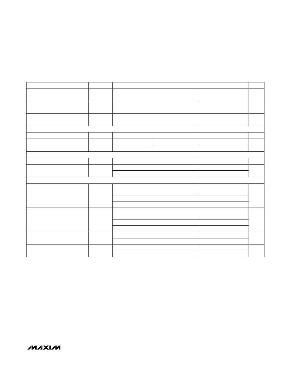
ELECTRICAL CHARACTERISTICS (continued)
(Circuit of Figure 1, no load on LDO, RTC, OUT1, OUT2, and REF, V
IN
= 12V, V
DD
= V
CC
= V
SECFB
= 5V, V
REFIN2
= 1.0V, BYP =
LDOSEL = GND, ONLDO = IN, ON1 = ON2 = V
CC
, T
A
= -40°C to +85°C, unless otherwise noted.) (Note 3)
PARAMETER
SYMBOL CONDITIONS
MIN
TYP
MAX
UNITS
OUT2 Undervoltage-Protection
Trip Threshold
V
UVP(OUT2)
With respect to error-comparator threshold
60
80
%
PGOOD2 Lower Trip Threshold
With respect to error-comparator threshold,
falling edge, hysteresis = 2%
-20 -10 %
PGOOD2 Output-Low Voltage
V
OUT2
= V
REFIN2
- 150mV (PGOOD2 low
impedance), I
SINK
= 4mA
0.4
V
CURRENT LIMIT
ILIM_ Adjustment Range
V
ILIM
0.2
2.0
V
R
ILIM
_ = 100k
40 60
Valley Current-Limit Threshold
(Adjustable)
V
VALLEY
V
AGND
- V
LX
_
R
ILIM
_ = 200k
85
115
mV
GATE DRIVERS
DH_ Gate Driver On-Resistance
R
DH
BST1 - LX1 and BST2 - LX2 forced to 5V
3.5
DL1, DL2; high state
4.5
DL_ Gate Driver On-Resistance
R
DL
DL1, DL2; low state
1.5
INPUTS AND OUTPUTS
High
V
CC
-
0.4V
REF or open
1.6
3.0
TON Input Logic Levels
Low
0.4
V
High (forced PWM)
V
CC
-
0.4V
Open (ultrasonic)
1.6
3.0
SKIP Input Logic Levels
Low (skip)
0.4
V
High (SMPS on)
2.4
ON_ Input Logic Levels
Low (SMPS off)
0.8
V
High (SMPS on)
2.4
ONLDO Input Logic Levels
Low (SMPS off)
0.8
V
Note 1: DC output accuracy specifications refer to the threshold of the error comparator. When the inductor is in continuous conduc-
tion, the MAX17101 regulates the valley of the output ripple, so the actual DC output voltage is higher than the trip level by
50% of the output ripple voltage. In discontinuous conduction (I
OUT
< I
LOAD(SKIP)
), the output voltage has a DC regulation
level higher than the error-comparator threshold by approximately 1.5% due to slope compensation.
Note 2: On-time and off-time specifications are measured from 50% point to 50% point at the DH pin with LX = PGND, VBST = 5V,
and a 500pF capacitor from DH to LX to simulate external MOSFET gate capacitance. Actual in-circuit times might be differ-
ent due to MOSFET switching speeds.
Note 3: Specifications to T
A
= -40°C are guaranteed by design and not production tested.
Note 4: Specifications increased by 1
Ω to account for test measurement error.