Rainbow Electronics MAX17101 User Manual
Page 2
MAX17101
Dual Quick-PWM, Step-Down Controller
with Low-Power LDO, RTC Regulator
2
_______________________________________________________________________________________
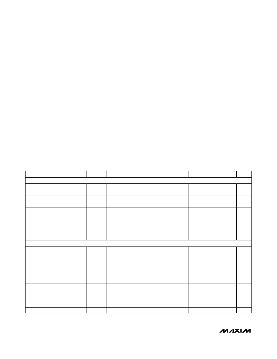
ABSOLUTE MAXIMUM RATINGS
ELECTRICAL CHARACTERISTICS
(Circuit of Figure 1, no load on LDO, RTC, OUT1, OUT2, and REF, V
IN
= 12V, V
DD
= V
CC
= V
SECFB
= 5V, V
REFIN2
= 1.0V, BYP =
LDOSEL = GND, ONLDO = IN, ON1 = ON2 = V
CC
, T
A
= 0°C to +85°C, unless otherwise noted. Typical values are at T
A
= +25°C.)
Stresses beyond those listed under “Absolute Maximum Ratings” may cause permanent damage to the device. These are stress ratings only, and functional
operation of the device at these or any other conditions beyond those indicated in the operational sections of the specifications is not implied. Exposure to
absolute maximum rating conditions for extended periods may affect device reliability.
IN, ONLDO to GND ................................................-0.3V to +28V
V
DD
, V
CC
to GND .....................................................-0.3V to +6V
RTC, LDO to GND ....................................................-0.3V to +6V
OUT_ to GND ...........................................................-0.3V to +6V
ON1, ON2 to GND....................................................-0.3V to +6V
PGOOD_ to GND........................................-0.3V to (V
CC
+ 0.3V)
REF, ILIM_, TON, SKIP to GND ..................-0.3V to (V
CC
+ 0.3V)
FB1, REFIN2, LDOSEL to GND ................................-0.3V to +6V
SECFB to GND .........................................................-0.3V to +6V
BYP to GND..............................................-0.3V to (V
LDO
+ 0.3V)
GND to PGND .......................................................-0.3V to +0.3V
DL_ to PGND ..............................................-0.3V to (V
DD
+ 0.3V)
BST_ to GND ..........................................................-0.3V to +34V
BST_ to V
DD
............................................................-0.3V to +28V
DH1 to LX1 ..............................................-0.3V to (V
BST1
+ 0.3V)
BST1 to LX1..............................................................-0.3V to +6V
DH2 to LX2 ..............................................-0.3V to (V
BST2
+ 0.3V)
BST2 to LX2..............................................................-0.3V to +6V
LDO, RTC, REF Short Circuit to GND.........................Momentary
RTC Current Continuous.....................................................+5mA
LDO Current (Internal Regulator)
Continuous..................................................................+100mA
LDO Current (Switched Over) Continuous .....................+200mA
Continuous Power Dissipation (T
A
= +70°C)
32-Pin 5mm x 5mm TQFN
(derate 34.5mW/°C above +70°C) .................................2.76W
Operating Temperature Range ...........................-40°C to +85°C
Junction Temperature ......................................................+150°C
Storage Temperature Range .............................-65°C to +150°C
Lead Temperature (soldering, 10s) .................................+300°C
PARAMETER
SYMBOL
CONDITIONS
MIN
TYP
MAX
UNITS
INPUT SUPPLIES
IN Standby Supply Current
I
IN(STBY)
V
IN
= 6V to 24V, ON1 = ON2 = GND,
ONLDO = V
CC
85
175
μA
IN Shutdown Supply Current
I
IN(SHDN)
V
IN
= 4.5V to 24V,
ON1 = ON2 = ONLDO = GND
50
70
μA
IN Supply Current
I
IN
ON1 = ON2 = REFIN2 = V
CC
,
SKIP = FB1 = GND,
V
OUT2
= 3.5V, V
OUT1
= 5.3V
0.1
0.2
mA
V
CC
Supply Current
I
CC
ON1 = ON2 = REFIN2 = V
CC
,
SKIP = FB1 = GND,
V
OUT2
= 3.5V, V
OUT1
= 5.3V
1.0
1.5
mA
PWM CONTROLLERS
5V preset output: FB1 = GND,
V
IN
= 12V,
SKIP = V
CC
4.925 5.00 5.075
V
OUT1
1.5V preset output: FB1 = V
CC
(5V),
V
IN
= 12V,
SKIP = V
CC
1.482 1.50 1.518
OUT1 Output-Voltage Accuracy
(Note 1)
V
FB1
Adjustable feedback output,
V
IN
= 12V,
SKIP = V
CC
0.690 0.700 0.710
V
OUT1 Voltage-Adjust Range
0.7
5.5
V
Low 0.04
0.110
FB1 Dual Mode™ Threshold
Voltage Levels
High
V
CC
-
1.6V
V
CC
-
0.7V
V
FB1 Input Bias Current
I
FB1
V
FB1
= 0.8V, T
A
= +25°C
-0.2
+0.2
μA
Dual Mode is a trademark of Maxim Integrated Products, Inc.