Detailed description, Pin description (continued) – Rainbow Electronics MAX4821 User Manual
Page 6
MAX4820/MAX4821
+3.3V/+5V, 8-Channel, Cascadable Relay Drivers
with Serial/Parallel Interface
6
_______________________________________________________________________________________
Detailed Description
The MAX4820/MAX4821 8-channel relay drivers offer
built-in kickback protection and drive +3.3V/+5V non-
latching or dual-coil-latching relays. These devices are
especially useful when driving +3V relays. Each inde-
pendent open-drain output features a 2
Ω on-resistance
and is guaranteed to sink 70mA (min) load current. Both
devices consume less than 50µA (max) quiescent cur-
rent and feature 1µA (min) output off-leakage current.
The MAX4820 features an SPI/QSPI/MICROWIRE-com-
patible serial interface. Input data is shifted into an 8-bit
shift register and latched to the outputs when CS transi-
tions from low to high. Each data bit in the shift register
corresponds to a specific output, allowing independent
control of all outputs.
The MAX4821 features a 4-bit (A0, A1, A2, LVL) parallel
input interface. The three bits (A0, A1, A2) determine
the output address, and LVL determines whether the
selected output is switched on or off. Data is latched to
the outputs when CS transitions from low to high.
Both devices feature separate set and reset functions
that allow the user to turn on or turn off all outputs
simultaneously with a single control line. Built-in hys-
teresis (Schmidt trigger) on all digital inputs allows this
device to be used with slow rising and falling signals,
such as those from optocouplers or RC power-up ini-
tialization circuits. The MAX4820/MAX4821 are avail-
able in 20-pin TSSOP and space-saving 20-pin thin
QFN packages.
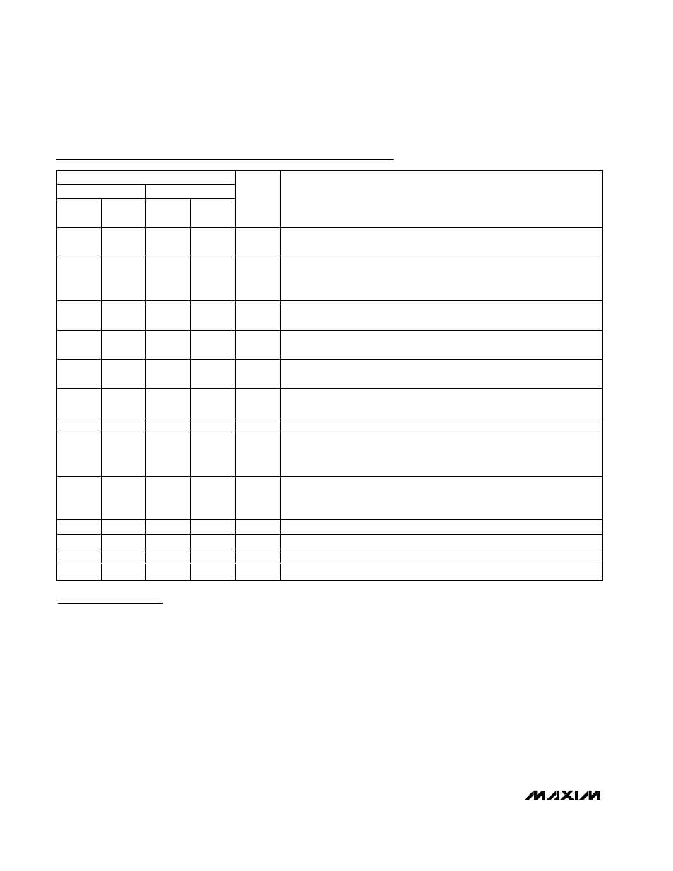
PIN
MAX4820
MAX4821
THIN
QFN
TSSOP
THIN
QFN
TSSOP
NAME
FUNCTION
12
14
12
14
OUT5
Open-Drain Output 5. Connect OUT5 to the low side of a relay coil. This
output is pulled to PGND when activated, but otherwise is high impedance.
13
15
13
15
COM
Common Free-Wheeling Diodes. Connect COM to V
CC
. COM can also be
connected to a separate supply that is higher than V
CC
. In that case, bypass
V
CC
to GND with a 0.1µF capacitor.
14
16
14
16
OUT4
Open-Drain Output 4. Connect OUT4 to the low side of a relay coil. This
output is pulled to PGND when activated, but otherwise is high impedance.
15
17
15
17
OUT3
Open-Drain Output 3. Connect OUT3 to the low side of a relay coil. This
output is pulled to PGND when activated, but otherwise is high impedance.
17
19
17
19
OUT2
Open-Drain Output 2. Connect OUT2 to the low side of a relay coil. This
output is pulled to PGND when activated, but otherwise is high impedance.
18
20
18
20
OUT1
Open-Drain Output 1. Connect OUT1 to the low side of a relay coil. This
output is pulled to PGND when activated, but otherwise is high impedance.
19
1
19
1
V
CC
Input Supply Voltage. Bypass V
CC
to GND with a 0.1µF capacitor.
20
2
20
2
SET
Set Input. Drive SET low to set all latches and registers high (all outputs are
turned on). SET overrides all parallel and serial control inputs. RESET
overrides SET under all conditions.
—
—
3
5
LVL
Level Input. LVL determines whether the selected address is switched on or
off. A logic high on LVL switches on the addressed output. A logic low on
LVL switches off the addressed output.
—
—
4
6
A0
Digital Address “0” Input. (See Table 2 for address mapping.)
—
—
5
7
A1
Digital Address “1” Input. (See Table 2 for address mapping.)
—
—
6
8
A2
Digital Address “2” Input. (See Table 2 for address mapping.)
—
—
—
—
EP
Exposed Pad. Solder exposed pad to GND.
Pin Description (continued)