Rainbow Electronics MAX4821 User Manual
Page 2
MAX4820/MAX4821
+3.3V/+5V, 8-Channel, Cascadable Relay Drivers
with Serial/Parallel Interface
2
_______________________________________________________________________________________
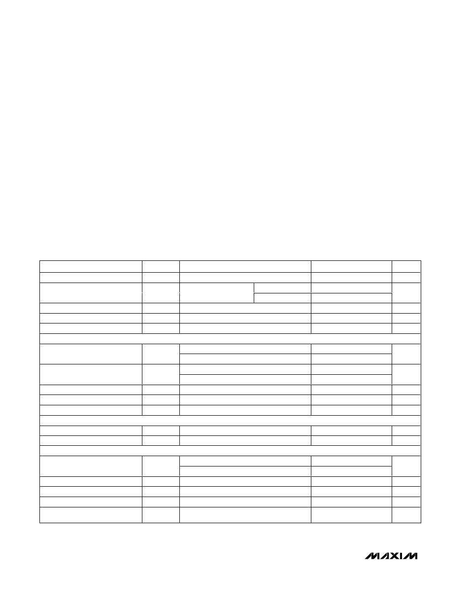
ABSOLUTE MAXIMUM RATINGS
ELECTRICAL CHARACTERISTICS
(V
CC
= +3V to +5.5V, V
COM
= V
CC
, T
A
= -40°C to +85°C, unless otherwise noted. Typical values are at T
A
= +25°C.) (Note 1)
Stresses beyond those listed under “Absolute Maximum Ratings” may cause permanent damage to the device. These are stress ratings only, and functional
operation of the device at these or any other conditions beyond those indicated in the operational sections of the specifications is not implied. Exposure to
absolute maximum rating conditions for extended periods may affect device reliability.
(All voltages referenced to GND.)
V
CC
, COM..............................................................-0.3V to +6.0V
OUT_........................................................-0.3V to (V
COM
+ 0.3V)
CS, SCLK, DIN, SET, RESET, A0, A1, A2, LVL......-0.3V to +6.0V
DOUT..........................................................-0.3V to (V
CC
+ 0.3V)
Continuous OUT_ Current (all outputs turned on) ............150mA
Continuous OUT_ Current (single output turned on) ........300mA
Continuous Power Dissipation (T
A
= +70°C)
20-Lead Thin QFN
(derate 16.9mW/°C above +70°C) .................................1350mW
θ
JA
.........................................................................59.3°C/W
20-Pin TSSOP
(derate 21.7mW/°C above +70°C) .................................1739mW
θ
JA
............................................................................46°C/W
Operating Temperature Range ...........................-40°C to +85°C
Junction Temperature ......................................................+150°C
Storage Temperature Range .............................-65°C to +150°C
Soldering Temperature (10s) ...........................................+300°C
PARAMETER
SYMBOL
CONDITIONS
MIN
TYP
MAX
UNITS
Operating Voltage
V
CC
2.3
5.5
V
V
CC
= 3.6V
15
50
Quiescent Current
I
Q
I
OUT
_ = 0,
logic inputs = 0 or V
CC
V
CC
= 5.5V
20
70
µA
Thermal Shutdown
160
°C
Power-On Reset
0.8
1.5
2.2
V
Power-On Reset Hysteresis
140
mV
DIGITAL INPUTS (SCLK, DIN, CS, LVL, A0, A1, A2, RESET, SET)
V
CC
= 3.3V
2.0
Input Logic High Voltage
V
IH
V
CC
= 5V
2.4
V
V
CC
= 3.3V
0.6
Input Logic Low Voltage
V
IL
V
CC
= 5V
0.8
V
Input Logic Hysteresis
V
HYST
150
mV
Input Leakage Currents
I
LEAK
Input voltages = 0 or 5.5V
-1.0
0.01
+1.0
µA
C
IN
Input Capacitance
C
IN
5
pF
DIGITAL OUTPUT (DOUT)
DOUT Low Voltage
V
OL
I
SINK
= 6mA
0.4
V
DOUT High Voltage
V
OH
I
SOURCE
= 0.5mA
V
CC
- 0.5
V
RELAY OUTPUT DRIVERS (OUT1–OUT8)
V
CC
= 2.7V
70
OUT_ Drive Current
V
CC
= 4.5V
70
mA
OUT_ On-Resistance
R
ON
V
CC
= 2.7V
2
6
Ω
OUT_ Voltage
V
OUT
_
V
CC
= 3.0V, I
OUT
_ = 70mA
0.4
V
I
OUT
Off-Leakage Current
I
LEAK
V
OUT
_ = V
CC
,
all outputs off
-1
+1
µA
Kickback Diode Forward Voltage
V
FORW
I
OUT
_ = 150mA (Note 2)
1.5
V