Electrical characteristics (continued) – Rainbow Electronics MAX4821 User Manual
Page 3
MAX4820/MAX4821
3.3V/+5V, 8-Channel, Cascadable Relay Drivers
with Serial/Parallel Interface
_______________________________________________________________________________________
3
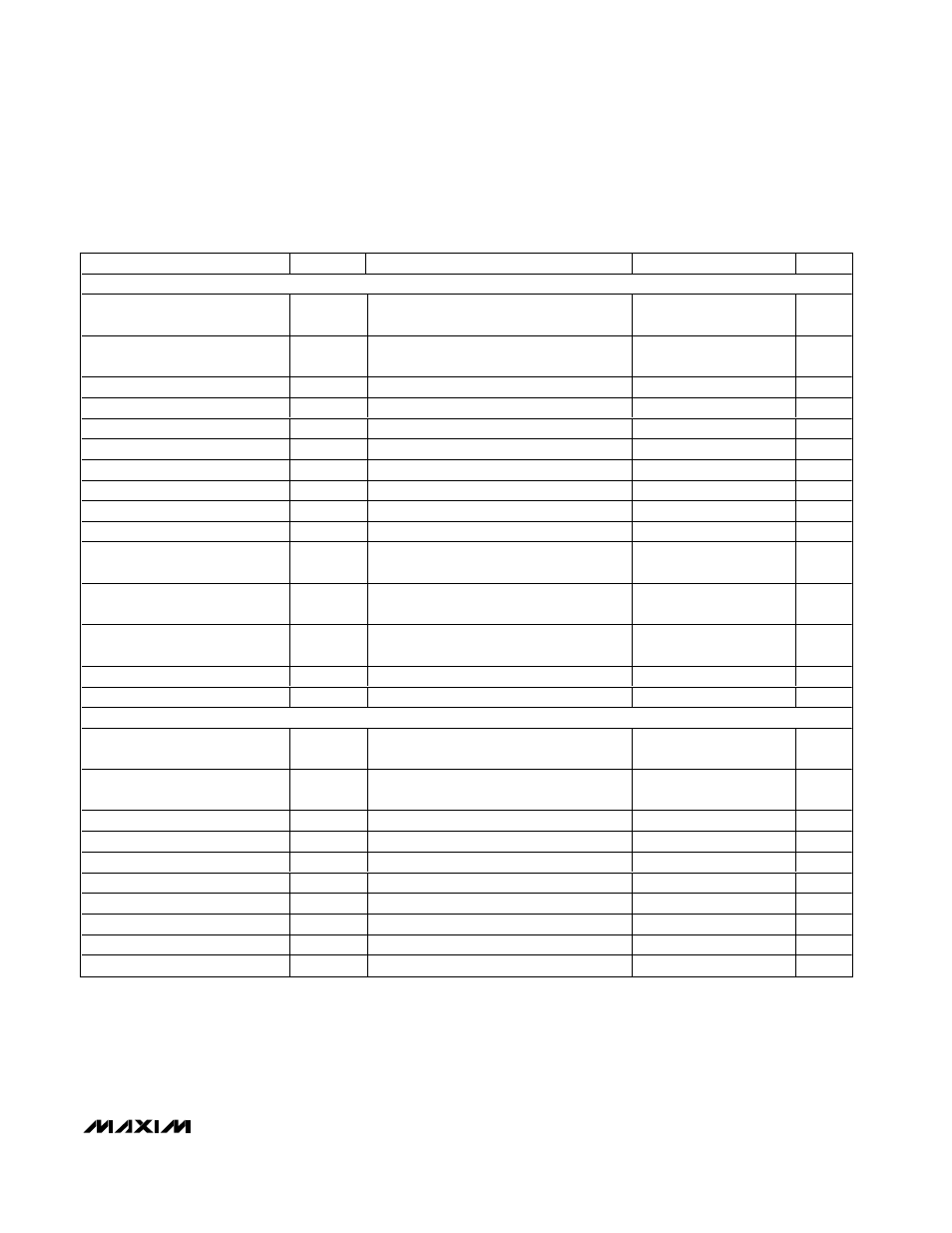
PARAMETER
SYMBOL
CONDITIONS
MIN
TYP
MAX
UNITS
SPI TIMING (MAX4821)
Turn-On Time (OUT_)
t
ON
From rising edge of CS, R
L
= 50
Ω,
C
L
= 50pF
1.0
µs
Turn-Off Time (OUT_)
t
OFF
From rising edge of CS, R
L
= 50
Ω,
C
L
= 50pF
1.0
µs
SCLK Frequency
f
SCLK
0
2.1
MHz
Cycle Time
t
CH
+ t
CL
480
ns
CS Fall to SCLK Rise Setup
t
CSS
240
ns
CS Rise to SCLK Hold
t
CSH
240
ns
SCLK High Time
t
CH
190
ns
SCLK Low Time
t
CL
190
ns
Data Setup Time
t
DS
100
ns
Data Hold Time
t
DH
0
ns
SCLK Fall to DOUT Valid
t
DO
50% of SCLK to 10% of DOUT,
C
L
= 50pF
85
120
ns
Rise Time (DIN, SCLK, CS, SET,
RESET)
t
SCR
20% of V
CC
to 70% of V
CC
, C
L
= 50pF
2
µs
Fall Time (DIN, SCLK, CS,
RESET, SET)
t
SCF
20% of V
CC
to 70% of V
CC
, C
L
= 50pF
2
µs
RESET Min Pulse Width
t
RW
70
ns
SET Min Pulse Width
t
SW
70
ns
PARALLEL TIMING (MAX4820)
Turn-On Time
t
ON
From rising edge of CS, R
L
= 50
Ω,
C
L
= 50pF
1
µs
Turn-Off Time
t
OFF
From rising edge of CS, R
L
= 50
Ω,
C
L
= 50pF
1
µs
LVL Setup Time
t
LS
100
ns
LVL Hold Time
t
LH
0
ns
Address to CS Setup Time
t
AH
100
ns
Address to CS Hold Time
t
AS
0
ns
Rise Time (A2, A1, A0, LVL)
t
SCR
20% of V
CC
to 70% of V
CC
, C
L
= 50pF
2
µs
Fall Time (A2, A1, A0, LVL)
t
SCF
20% of V
CC
to 70% of V
CC
, C
L
= 50pF
2
µs
RESET Pulse Width
t
RW
70
ns
SET Pulse Width
t
SW
70
ns
ELECTRICAL CHARACTERISTICS (continued)
(V
CC
= +3V to +5.5V, V
COM
= V
CC
, T
A
= -40°C to +85°C, unless otherwise noted. Typical values are at T
A
= +25°C.) (Note 1)
Note 1: Specifications at -40°C are guaranteed by design and not production tested.
Note 2: After relay turn-off, inductive kickback may momentarily cause the voltage at OUT_ to exceed V
COM
. This is considered part
of normal operation and will not damage the device.