Pin description (continued) – Rainbow Electronics MAXQ3120 User Manual
Page 7
MAXQ3120
High-Precision ADC
Mixed-Signal Microcontroller
_____________________________________________________________________
7
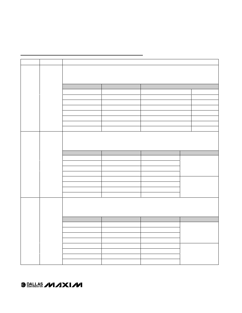
Pin Description (continued)
PIN
NAME
FUNCTION
General-Purpose, Digital, I/O, Type-D Port; External Edge-Selectable Interrupt. These port pins
function as bidirectional I/O pins only. All port pins default to input mode with weak pullups enabled
after a reset. Port pins P0.3, P0.4, and P0.5 can be configured as external interrupt inputs. All alternate
functions must be enabled from software.
PIN
PORT
ALTERNATE FUNCTIONS
64
P0.0
RTC Square-Wave Output
—
65
P0.1
Serial Port 0 Receive
—
66
P0.2
Serial Port 0 Transmit
—
67
P0.3
Timer 0 Gate Input
INT0
68
P0.4
Timer 0 Input
INT1
69
P0.5
Timer 1 Input/Output
INT2
70
P0.6
Timer 2 Input/Output A (T2P)
—
64–71
P0.0–P0.7/
SQW, RXD0,
TXD0,
INT0–INT2/
T2A, T2B/
T0G, T0, T1
71
P0.7
Timer 2 Input/Output B (T2PB)
—
G e n e r a l - Pu r p o s e , 8 - B i t , D i g i t a l , I/ O , T y p e - C Po r t ; LC D Se g m e n t - D r iv e r Ou t p u t . These p or t p i ns
functi on as b oth b i d i r ecti onal I/O p i ns and LC D seg m ent- d r i ve outp uts. Al l p or t p i ns d efaul t to i np ut m od e
w i th w eak p ul l up s enab l ed after a r eset. S etti ng the LC D enab l e ( P C Fx) b i t for a g r oup of four p or t p i ns
enab l es the LC D functi on and d i sab l es the g ener al - p ur p ose I/O functi on on al l p i ns i n that g r oup .
PIN
PORT
LCD SEGMENT
LCD ENABLE
76
P1.0
SEG19
77
P1.1
SEG18
78
P1.2
SEG17
79
P1.3
SEG16
PCF1
80
P1.4
SEG15
1
P1.5
SEG14
2
P1.6
SEG13
76–80, 1,
2, 3
P1.0–P1.7/
SEG19–
SEG12
3
P1.7
SEG12
PCF0
G e n e r a l - Pu r p o s e , 8 - B i t , D i g i t a l , I/ O , T y p e - C Po r t ; LC D Se g m e n t - D r iv e r Ou t p u t . These p or t p i ns
functi on as b oth b i d i r ecti onal I/O p i ns and LC D seg m ent- d r i ve outp uts. Al l p or t p i ns d efaul t to i np ut m od e
w i th w eak p ul l up s enab l ed after a r eset. S etti ng the LC D enab l e ( P C Fx) b i t for a g r oup of four p or t p i ns
enab l es the LC D functi on and d i sab l es the g ener al - p ur p ose I/O functi on on al l p i ns i n that g r oup .
PIN
PORT
LCD SEGMENT
LCD ENABLE
28
P2.0
SEG20
29
P2.1
SEG21
30
P2.2
SEG22
31
P2.3
SEG23
PCF2
32
P2.4
SEG24
33
P2.5
SEG25
34
P2.6
SEG26
28–34, 39
P2.0–P2.7/
SEG20–
SEG27
39
P2.7
SEG27
PCF3