High-speed hardware multiplier – Rainbow Electronics MAXQ3120 User Manual
Page 23
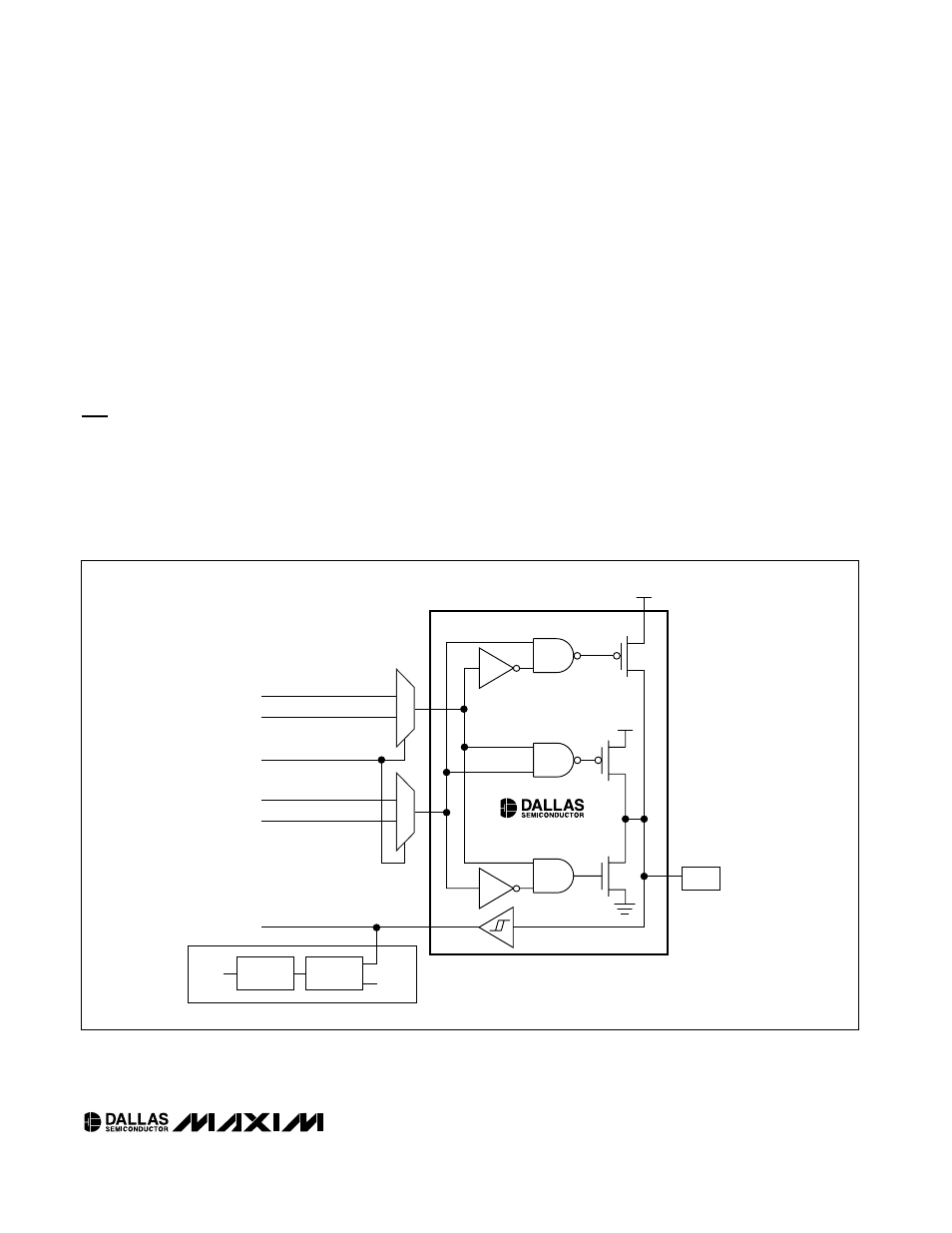
Type C port pins have Schmitt Trigger receivers and
full CMOS output drivers, and can support alternate
functions. The pin is either tri-stated or a weak pullup
when defined as an input, dependent on the state of
the corresponding bit in the output register.
Type D port pins have Schmitt Trigger receivers and
full CMOS output drivers, and can support alternate
functions. The pin is either tri-stated or a weak pullup
when defined as an input, dependent on the state of
the corresponding bit in the output register. All Type D
pins also have interrupt capability.
High-Speed Hardware Multiplier
The hardware multiplier module performs high-speed
multiply, square, and accumulate operations, and can
complete a 16-bit x 16-bit multiply-and-accumulate
operation in a single cycle. The hardware multiplier
consists of two 16-bit parallel-load operand registers
(MA, MB), a 40-bit accumulator that is formed by three
16-bit parallel registers (MC2, MC1, and MC0), and a
status/control register (MCNT). Loading the registers
can automatically initiate the operation, saving time on
repetitive calculations. The accumulate function of the
hardware multiplier is an essential element of digital fil-
tering, signal processing, and proportional/integral/
derivative (PID) algorithm-based control systems.
The hardware multiplier module supports the following
operations:
• Multiply unsigned (16 bit x 16 bit)
• Multiply signed (16 bit x 16 bit)
• Multiply-accumulate unsigned (16 bit x 16 bit)
• Multiply-accumulate signed (16 bit x 16 bit)
• Square unsigned (16 bit)
• Square signed (16 bit)
• Square-accumulate unsigned (16 bit)
• Square-accumulate signed (16 bit)
MAXQ3120
High-Precision ADC
Mixed-Signal Microcontroller
____________________________________________________________________
23
MAXQ3120
PD.x
SF DIRECTION
SF ENABLE
MUX
MUX
PO.x
V
DDIO
SF OUTPUT
V
DDIO
WEAK
I/O PAD
PORT PIN
INTERRUPT
FLAG
FLAG
PI.x OR SF INPUT
EIES.x
TYPE D PORT ONLY
DETECT
CIRCUIT
Figure 3. Type C/D Port Pin Schematic