Pin description – Rainbow Electronics MAXQ3120 User Manual
Page 6
MAXQ3120
High-Precision ADC
Mixed-Signal Microcontroller
6
_____________________________________________________________________
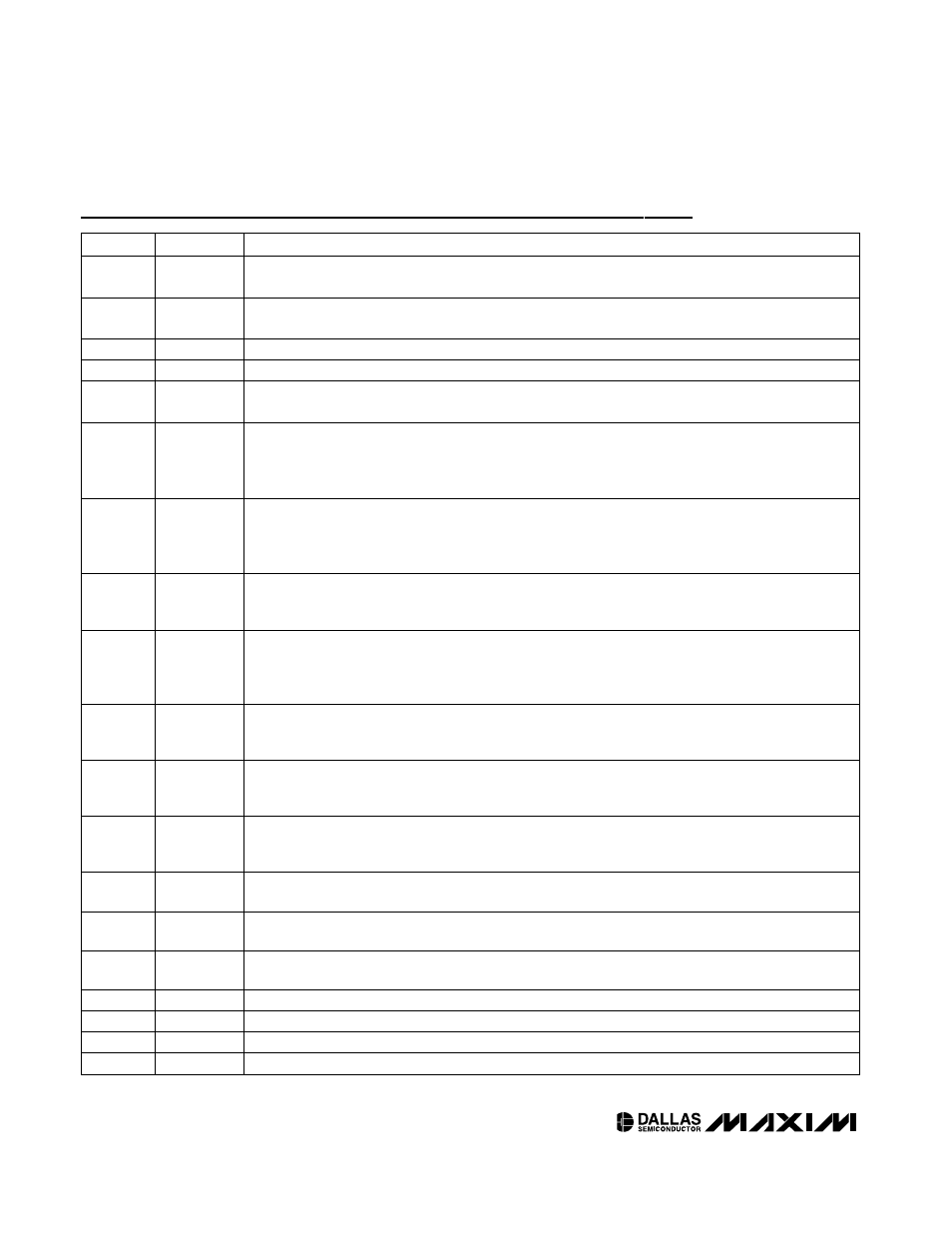
Pin Description
PIN
NAME
FUNCTION
22, 38,
60, 74
DV
DD
Digital Supply Voltage (+3.3V)
19, 37, 43,
59, 75
DGND
Digital Ground
44
AV
DD
Analog Supply Voltage
52
AGND
Analog Ground
12
V
LCD
LCD Bias-Control Voltage. Highest LCD drive voltage used in all bias modes. This pin must be
connected to an external supply when using the LCD display controller.
13
V
LCD1
LCD Bias, Voltage 1. Next highest LCD drive voltage, used in 1/2 and 1/3 LCD bias modes. An internal
resistor-divider sets the voltage at this pin. External resistors and capacitors can be used to change
LCD voltage or drive capability at this pin. This pin must be shunted externally to V
LCD2
when using 1/2
bias mode.
14
V
LCD2
LCD Bias, Voltage 2. Third highest LCD drive voltage, used in 1/3 LCD bias mode only. An internal
resistor-divider sets the voltage at this pin. External resistors and capacitors can be used to change
LCD voltage or drive capability at this pin. This pin must be shunted externally to V
LCD1
when using
1/2 bias mode.
15
V
ADJ
LCD Adjustment Voltage. Lowest LCD drive voltage, used in all bias modes. Connect to DGND
through an external resistor to provide external control of the LCD contrast. Leave disconnected for
internal contrast adjustment.
63
RESET
Digital, Active-Low, Reset Input/Output. The CPU is held in reset when this is low and begins
executing from the reset vector when released. The pin includes a pullup current source and should be
driven by an open-drain, external source capable of sinking in excess of 2mA. This pin is driven low as
an output when an internal reset condition occurs.
20
HFXIN
High-Frequency Crystal Input. Connect an external crystal between HFXIN and HFXOUT to generate
the high-frequency system clock. HFXIN and HFXOUT contain integral 16pF load capacitors, so no
external capacitor is required.
21
HFXOUT
High-Frequency Crystal Output. Connect an external crystal between HFXIN and HFXOUT to
generate the high-frequency system clock. HFXIN and HFXOUT contain integral 16pF load capacitors,
so no external capacitor is required.
53
V
BAT
Digital Battery-Backup Supply. This supply provides an optional battery backup for the RTC when
DV
DD
power is removed. If this supply is not provided, all functions of the device operate as normal,
but the RTC is cleared upon power-on reset (POR).
61
32KIN
32kHz Crystal Input. Connect an external, 32kHz watch crystal between 32KIN and 32KOUT to
generate the 32kHz system clock. This clock is required for the RTC to operate.
62
32KOUT
32kHz Crystal Output. Connect an external, 32kHz watch crystal between 32KIN and 32KOUT to
generate the 32kHz system clock. This clock is required for the RTC to operate.
51
V
REF
Voltage Reference Input/Output. Bias voltage (+1.25V) for the ADCs. An external reference voltage
can be connected to this pin when extremely high accuracy is required.
45
AN0-
Negative Input for Sigma-Delta ADC Channel 0
46
AN0+
Positive Input for Sigma-Delta ADC Channel 0
47
AN1-
Negative Input for Sigma-Delta ADC Channel 1
48
AN1+
Positive Input for Sigma-Delta ADC Channel 1