Rainbow Electronics MAXQ3120 User Manual
Page 2
MAXQ3120
High-Precision ADC
Mixed-Signal Microcontroller
2
_____________________________________________________________________
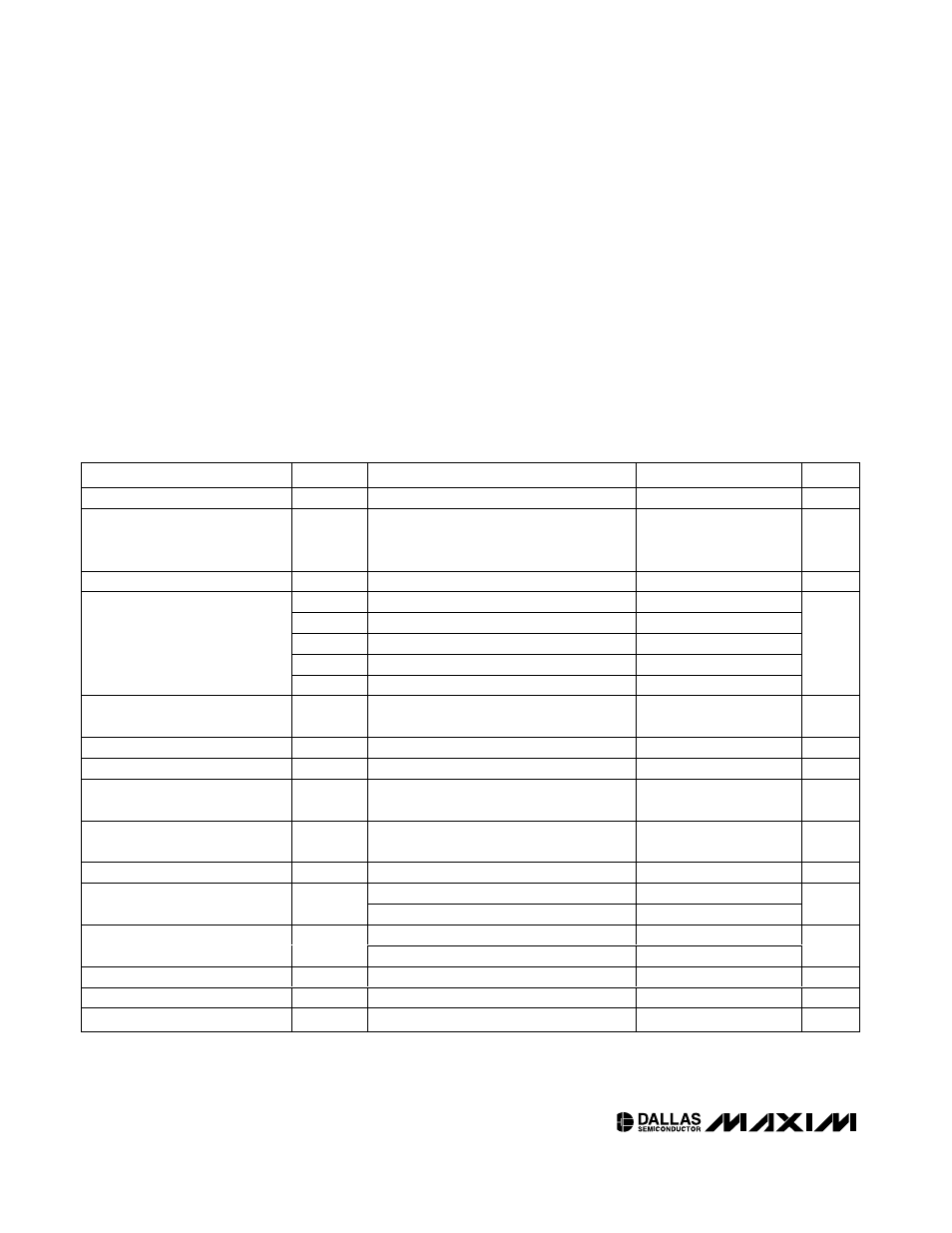
ABSOLUTE MAXIMUM RATINGS
ELECTRICAL CHARACTERISTICS
(DV
DD
, AV
DD
= V
RST
to 3.6V, V
REF
= 1.25V (external), f
HFXIN
= 8MHz, T
A
= -40°C to +85°C, unless otherwise noted.) (Note 1)
Stresses beyond those listed under “Absolute Maximum Ratings” may cause permanent damage to the device. These are stress ratings only, and functional
operation of the device at these or any other conditions beyond those indicated in the operational sections of the specifications is not implied. Exposure to
absolute maximum rating conditions for extended periods may affect device reliability.
Voltage Range on DV
DD
Relative to DGND ..........-0.3V to +4.0V
Voltage Range on AV
DD
Relative to AGND...........-0.3V to +4.0V
Voltage Range on AGND Relative to DGND .........-0.3V to +0.3V
Voltage Range on AV
DD
Relative to DV
DD
............-0.3V to +0.3V
Voltage Range on Any Pin Relative to DGND
Except AN0+, AN0-, AN1+, AN1-.........-0.3V to (DV
DD
+ 0.5V)
Voltage Range on AN0+, AN0-, AN1+,
AN1- Relative to AGND ......................................-4.0V to +4.0V
Operating Temperature Range ...........................-40°C to +85°C
Junction Temperature ......................................................+150°C
Storage Temperature Range .............................-65°C to +150°C
Soldering Temperature .......................................See IPC/JEDEC
J-STD-020 Specification
PARAMETER
SYMBOL
CONDITIONS
MIN
TYP
MAX
UNITS
Digital Supply Voltage
DV
DD
V
RST
3.3
3.6
V
Digital Supply Ramp Rate
Can be controlled by placing a 1µF or
higher capacitor between DV
DD
and
ground
-16
+16
V/ms
Digital Power-Fail Reset
V
RST
2.8
2.9
3.03
V
I
DD1
/1 mode
21
28
I
DD2
/2 mode
11
I
DD3
/4 mode
5.7
I
DD4
/8 mode
3.1
Active Current
(Note 2)
I
DD5
PMM mode
1.0
mA
Stop-Mode Current
(DV
DD
plus AV
DD
)
I
STOP
320
760
µA
Battery Supply Voltage
V
BAT
1.8
3.8
V
Battery Current
I
BAT
RTCE = 1, DV
DD
= 0V, V
BAT
= 3.6V
5.1
10
µA
Input High Voltage
V
IH
0.7 x
DV
DD
DV
DD
+ 0.3
V
Input Low Voltage
V
IL
-0.3
0.3 x
DV
DD
V
Input Hysteresis (Schmitt)
V
IHYS
0.6
V
I
OH
= +1.5mA
DV
DD
- 0.4
Output High Voltage
(All Ports)
V
OH
I
OH
= +2.5mA
DV
DD
- 0.5
V
I
OL
= 3mA sink current
0.4
Output Low Voltage (All Ports,
RESET)
V
OL
I
OL
= 3.65mA sink current
0.5
V
Input Low Current (All Ports)
I
IL
V
IL
= 0.4V; weak pullup enabled
-50
µA
RESET Pullup Resistance
R
RST
50
100
200
k
Ω
Input Leakage (All Ports)
I
L
Weak pullup disabled
-1
+1
µA