Pin description, Typical operating characteristics (continued) – Rainbow Electronics MAX16834 User Manual
Page 6
Pin Description
PIN
NAME
FUNCTION
1
OVP+
LED-String Overvoltage Protection Input. Connect a resistive voltage-divider between the positive
output, OVP+, and LV to set the overvoltage threshold. OVP+ has a 1.435V threshold voltage with a
200mV hysteresis.
2
SGND
Signal Ground
3
COMP
Error-Amplifier Output. Connect an RC network from COMP to SGND for stable operation. See the
Feedback Compensation section.
4
REF
3.7V Reference Output Voltage. Bypass REF to SGND with a 0.1µF to 0.22µF ceramic capacitor.
5
REFI
Current Reference Input. V
REFI
provides a reference voltage for the current-sense amplifier to set the
LED current.
6
SC
Current-Mode Slope Compensation Setting. Connect to an appropriate external capacitor from SC to
SGND to generate a ramp signal for stable operation.
MAX16834
High-Power LED Driver with Integrated High-Side LED
Current Sense and PWM Dimming MOSFET Driver
6
_______________________________________________________________________________________
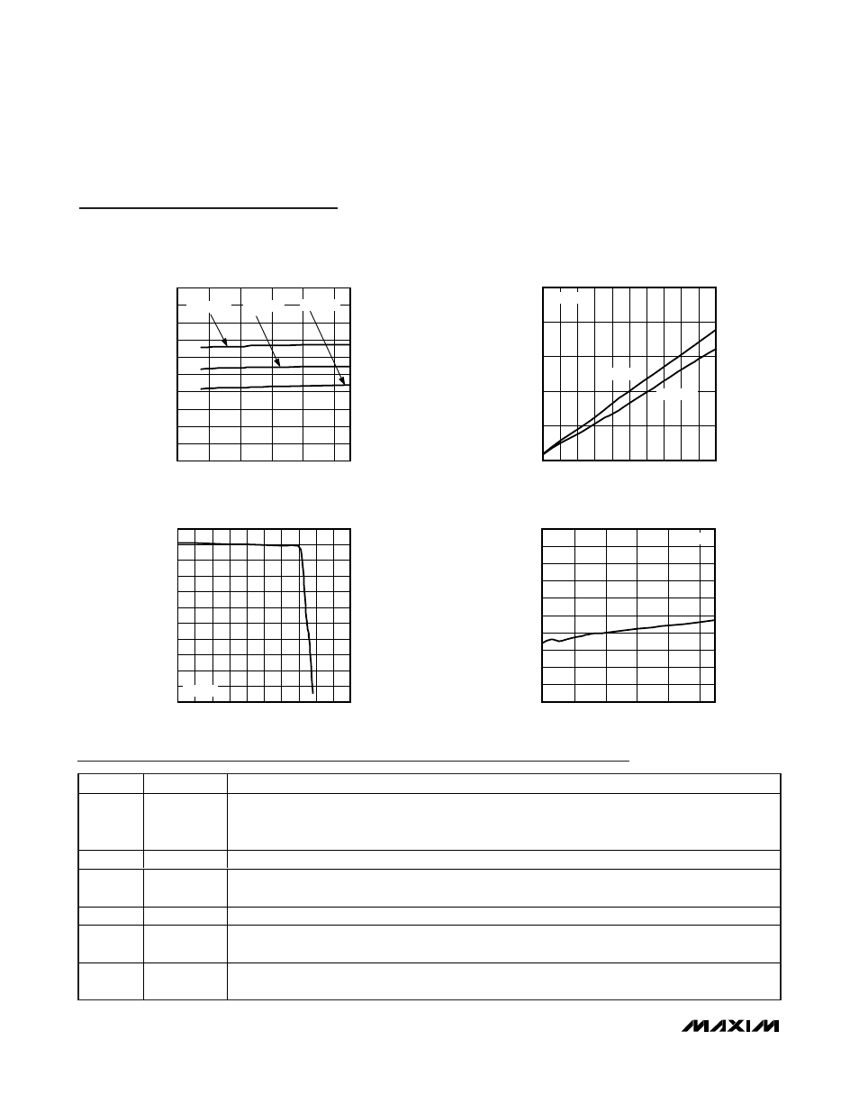
Typical Operating Characteristics (continued)
(V
IN
= V
HV
= 12V, V
UVEN
= 5V, V
LV
= V
PWMDIM
= SGND, C
VCC
= 4.7µF, C
LCV
= 100nF, C
REF
= 100nF, R
SENSE+
= 0.1
Ω,
R
RT
= 10k
Ω, T
A
= +25°C, unless otherwise noted.)
V
CC
vs. V
IN
MAX16834 toc10
V
IN
(V)
V
CC
(V)
26
22
18
14
10
7.02
7.04
7.06
7.08
7.10
7.12
7.14
7.16
7.18
7.20
7.00
6
T
A
= +125
°C
T
A
= +25
°C
T
A
= -40
°C
NDRV RISE/FALL TIME
vs. CAPACITANCE
MAX16834 toc11
CAPACITANCE (nF)
NDRV RISE TIME (ns)
9
8
7
6
5
4
3
2
1
10
20
30
40
50
0
0
10
V
IN
= 12V
RISE TIME
FALL TIME
V
CLV
vs. V
HV
MAX16834 toc13
V
HV
(V)
V
CLV
(V)
26
22
18
14
10
5.01
5.02
5.03
5.04
5.05
5.06
5.07
5.08
5.09
5.10
5.00
6
V
IN
= 12V
V
CLV
vs. I
CLV
MAX16834 toc12
I
CLV
(mA)
V
CLV
(V)
4.5
4.0
3.0 3.5
1.0 1.5 2.0 2.5
0.5
0.50
1.00
1.50
2.00
2.50
3.00
3.50
4.00
4.50
5.00
5.50
0
0
5.0
V
IN
= 12V