Rainbow Electronics MAX16834 User Manual
Page 2
MAX16834
High-Power LED Driver with Integrated High-Side LED
Current Sense and PWM Dimming MOSFET Driver
2
_______________________________________________________________________________________
ABSOLUTE MAXIMUM RATINGS
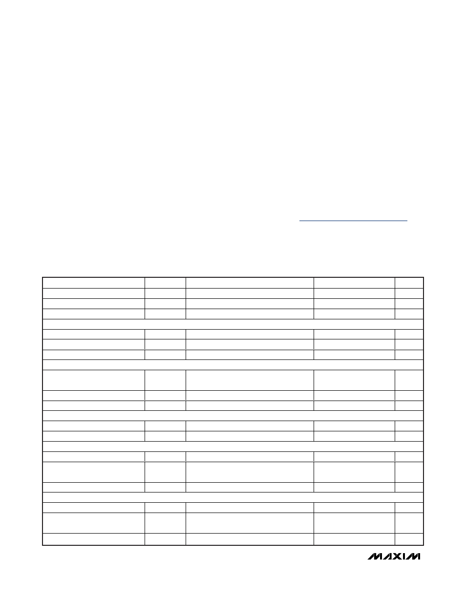
ELECTRICAL CHARACTERISTICS
(V
IN
= V
HV
= 12V, V
UVEN
= 5V, V
LV
= V
PWMDIM
= SGND, C
VCC
= 4.7µF, C
LCV
= 100nF, C
REF
= 100nF, R
SENSE+
= 0.1
Ω,
R
RT
= 10k
Ω, T
A
= T
J
= -40°C to +125°C, unless otherwise noted. Typical values are at T
A
= +25°C.)
Stresses beyond those listed under “Absolute Maximum Ratings” may cause permanent damage to the device. These are stress ratings only, and functional
operation of the device at these or any other conditions beyond those indicated in the operational sections of the specifications is not implied. Exposure to
absolute maximum rating conditions for extended periods may affect device reliability.
Note 1: Package thermal resistances were obtained using the method described in JEDEC specification JESD51-7, using a four-
layer board. For detailed information on package thermal considerations, refer to
www.maxim-ic.com/thermal-tutorial
.
IN, HV, LV to SGND................................................-0.3V to +30V
OVP+, SENSE+, DIMOUT, CLV to SGND ..............-0.3V to +30V
SENSE+ to LV........................................................-0.3V to +0.3V
HV, IN to LV ............................................................-0.3V to +30V
OVP+, CLV, DIMOUT to LV ......................................-0.3V to +6V
PGND to SGND .....................................................-0.3V to +0.3V
V
CC
to SGND ..........................................................-0.3V to +12V
NDRV to PGND...........................................-0.3V to (V
CC
+ 0.3V)
All Other Pins to SGND.............................................-0.3V to +6V
NDRV Continuous Current................................................±50mA
DIMOUT Continuous Current..............................................±2mA
V
CC
Short-Circuit Current to SGND Duration ...........................1s
Continuous Power Dissipation (T
A
= +70°C)
20-Pin TQFN 4mm x 4mm
(derate 25.6mW/°C* above +70°C) ............................2051mW
Junction-to-Ambient Thermal Resistance (
θ
JA
) (Note 1).....39°C/W
Junction-to-Case Thermal Resistance (
θ
JC
) (Note 1) ........6°C/W
Operating Temperature Range .........................-40°C to +125°C
Junction Temperature ......................................................+150°C
Storage Temperature Range .............................-65°C to +150°C
Lead Temperature (soldering, 10s) .................................+300°C
*
As per JEDEC51 standard (multilayer board).
PARAMETER
SYMBOL
CONDITIONS
MIN
TYP
MAX
UNITS
Input Voltage Range
V
IN
4.75
28
V
Quiescent Supply Current
I
Q
Excluding I
LED
6
10
mA
Shutdown Supply Current
I
SHDN
V
UVEN
= 0
30
60
µA
INTERNAL LINEAR REGULATOR (V
CC
)
Output Voltage
V
CC
0
≤ I
CC
≤ 50mA, 9.5V ≤ V
IN
≤ 28V
6.3
7
7.7
V
Dropout Voltage
V
OD
I
CC
= 35mA (Note 2)
0.65
1.8
V
Short-Circuit Current
V
CC
= 0V, V
IN
= 12V
80
300
mA
LINEAR REGULATOR (CLV)
Output Voltage
(V
CLV -
V
LV
)
0
≤ I
CLV
≤ 2mA, 6V ≤ V
HV
≤ 28V,
6V
≤ V
(HV-LV)
≤ 22V
4.7
5
5.3
V
Dropout Voltage
V
DO
I
CLV
= 2mA, 0
≤ V
LV
≤ 23.3V (Note 3)
0.5
V
Short-Circuit Current
V
CLV
= 12V, V
IN
= 12V, V
HV
= 24V
2.2
10
mA
REFERENCE VOLTAGE (REF)
Output Voltage
V
REF
0
≤ I
REF
≤ 1mA, 4.75V ≤ V
IN
≤ 28V
3.625
3.70
3.775
V
REF Short-Circuit Current
V
REF
= 0
30
mA
UNDERVOLTAGE LOCKOUT/ENABLE INPUT (UVEN)
UVEN On Threshold Voltage
V
UVEN_THUP
1.395
1.435
1.475
V
UVEN Threshold Voltage
Hysteresis
200
mV
Input Leakage Current
I
LEAK
V
UVEN
= 0
I1I
µA
PWMDIM
PWMDIM On Threshold Voltage
V
PWMDIM
1.395
1.435
1.475
V
PWMDIM Threshold Voltage
Hysteresis
200
mV
Input Leakage Current
V
PWMDIM
= 0
I1I
µA