Rainbow Electronics MAX9768 User Manual
Page 2
MAX9768
10W Mono Class D Speaker
Amplifier with Volume Control
2
_______________________________________________________________________________________
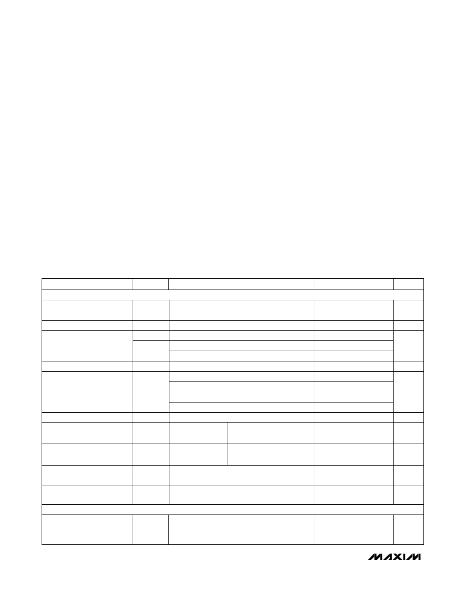
ABSOLUTE MAXIMUM RATINGS
ELECTRICAL CHARACTERISTICS
(PV
DD
= 12V, V
DD
= 3.3V, GND = PGND = 0V, V
SHDN
= V
DD
, V
MUTE
= 0V; Max volume setting; speaker load resistor connected
between OUT+ and OUT-, R
L
=
∞, unless otherwise noted. C
BIAS
= 2.2µF, C1 = C2 = 0.1µF, C
IN
= 0.47µF, R
IN
= 20k
Ω, R
F
= 30kΩ,
SSM mode. Filterless modulation mode (see the
Functional Diagram/Typical Application Circuit). T
A
= T
MIN
to T
MAX
, unless otherwise
noted. Typical values are at T
A
= +25°C.) (Note 1)
Stresses beyond those listed under “Absolute Maximum Ratings” may cause permanent damage to the device. These are stress ratings only, and functional
operation of the device at these or any other conditions beyond those indicated in the operational sections of the specifications is not implied. Exposure to
absolute maximum rating conditions for extended periods may affect device reliability.
PV
DD
to PGND........................................................-0.3V to +16V
V
DD
to GND ..............................................................-0.3V to +4V
SCLK, SDA/VOL to GND ..........................................-0.3V to +4V
FB, SYNCOUT ............................................-0.3V to (V
DD
+ 0.3V)
BOOT_ to OUT_........................................................-0.3V to +4V
OUT_ to GND ...........................................-0.3V to (PV
DD
+ 0.3V)
PGND to GND ......................................................-0.3V to +0.3V
Any Other Pin to GND ..............................................-0.3V to +4V
OUT_ Short-Circuit Duration.......................................Continuous
Continuous Current (PV
DD
, PGND, OUT_) ..........................2.2A
Continuous Input Current (Any Other Pin) .......................±20mA
Continuous Input Current (FB_) .......................................±60mA
Continuous Power Dissipation (T
A
= +70°C)
Single-Layer Board:
24-Pin Thin QFN 4mm x 4mm,
(derate 20.8mW/°C above +70°C) .................................1.67W
Multilayer Board:
24-Pin Thin QFN 4mm x 4mm,
(derate 27.8mW/°C above +70°C) .................................2.22W
θ
JA
, Single-Layer Board…...........................................….48°C/W
θ
JA
, Multilayer Board ...................................................….36°C/W
Operating Temperature Range ...........................-40°C to +85°C
Storage Temperature Range .............................-65°C to +150°C
Lead Temperature (soldering, 10s) ................................+300°C
PARAMETER
SYMBOL
CONDITIONS
MIN
TYP
MAX
UNITS
GENERAL
Speaker Supply Voltage
Range
PV
DD
Inferred from PSRR test
4.5
14.0
V
Supply Voltage Range
V
DD
Inferred from PSRR and UVLO test
2.7
3.6
V
I
VDD
7
14.2
Filterless modulation
4
7.6
Quiescent Current
I
PVDD
Classic PWM modulation
4
7.6
mA
Shutdown Current
I
SHDN
I
SHDN
= I
PVDD
+ I
DD
,
SHDN = GND
0.5
50
µA
Filterless modulation, V
MUTE
= V
DD
, T
A
= +25°C
±2
±12.5
Output Offset
V
OS
Filterless modulation, V
MUTE
= 0V, T
A
= +25°C
±2
±14
mV
MAX9768
220
Turn-On Time
t
ON
MAX9768B
15
ms
Common-Mode Bias Voltage
V
BIAS
1.5
V
Input Amplifier Output-
Voltage Swing High
V
OH
Specified as
V
DD
- V
OH
R
L
= 2k
Ω connect to 1.5V
3.6
100
mV
Input Amplifier Output-
Voltage Swing Low
V
OL
Specified as
V
OL
- GND
R
L
= 2k
Ω connect to 1.5V
6
50
mV
Input Amplifier Output
Short-Circuit Current Limit
±60
mA
Input Amplifier Gain-
Bandwidth Product
GBW
1.8
MHz
SPEAKER AMPLIFIERS
Internal Gain
A
VMAX
Max volume setting; from FB to amplifier outputs
|(OUT+) - (OUT-)|; excludes external gain
resistors
29.27
30.1
31.00
dB