Pin description – Rainbow Electronics MAX9768 User Manual
Page 11
MAX9768
10W Mono Class D Speaker
Amplifier with Volume Control
______________________________________________________________________________________
11
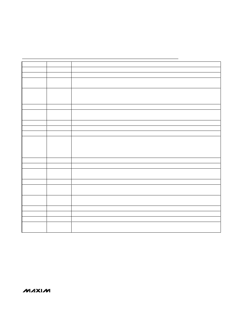
Pin Description
PIN
NAME
FUNCTION
1, 2
OUT+
Positive Speaker Output
3, 16
PV
DD
Speaker Amplifier Power-Supply Input. Bypass with a 1µF capacitor to ground.
4
BOOT+
Positive Speaker Output Boost Flying-Capacitor Connection. Connect a 0.1µF ceramic capacitor
between BOOT+ and OUT+.
5
SCLK
I
2
C Serial-Clock Input and Modulation Scheme Select. In I
2
C mode (ADDR1 and ADDR2
≠ GND)
acts as I
2
C serial-clock input. When ADDR1 and ADDR2 = GND. Connect SCLK to V
DD
for classic
PWM modulation, or connect SCLK to ground for filterless modulation.
6
SDA/VOL
I
2
C Serial Data I/O and Analog Volume Control Input
7
FB
Feedback. Connect feedback resistor between FB and IN to set amplifier gain. See the Adjustable
Gain section.
8
IN
Audio Input
9, 11
GND
Ground
10
BIAS
Common-Mode Bias Voltage. Bypass with a 2.2µF capacitor to GND.
12
SYNC
Frequency Select and External Clock Input.
SYNC = GND: Fixed-frequency mode with f
S
= 1200kHz.
SYNC = Unconnected: Fixed-frequency mode with f
S
= 1440kHz.
SYNC = V
DD
: Spread-spectrum mode with f
S
= 1200kHz ±30kHz.
SYNC = Clocked: Fixed-frequency mode with f
S
= external clock frequency.
13
SYNCOUT
Clock Signal Output
14
V
DD
Power-Supply Input. Bypass with a 1µF capacitor to GND.
15
BOOT-
Negative Speaker Output Boost Flying-Capacitor Connection. Connect a 0.1µF ceramic capacitor
between BOOTL- and OUTL-.
17, 18
OUT-
Negative Speaker Output
19
SHDN
Shutdown Input. Drive
SHDN low to disable the audio amplifiers. Connect SHDN to V
DD
for normal
operation
20
MUTE
Mute Input. Drive MUTE high to mute the speaker outputs. Connect MUTE to GND for normal
operation.
21, 22
PGND
Power Ground
23
ADDR2
Address Select Input 2. I
2
C address option, also selects volume control mode.
24
ADDR1
Address Select Input 1. I
2
C address option, also selects volume control mode.
EP
EP
Exposed Pad. Connect the exposed thermal pad to GND, and use multiple vias to a solid copper
area on the bottom of the PCB.