Pin description – Rainbow Electronics MAX9217 User Manual
Page 5
MAX9217
27-Bit, 3MHz-to-35MHz
DC-Balanced LVDS Serializer
_______________________________________________________________________________________
5
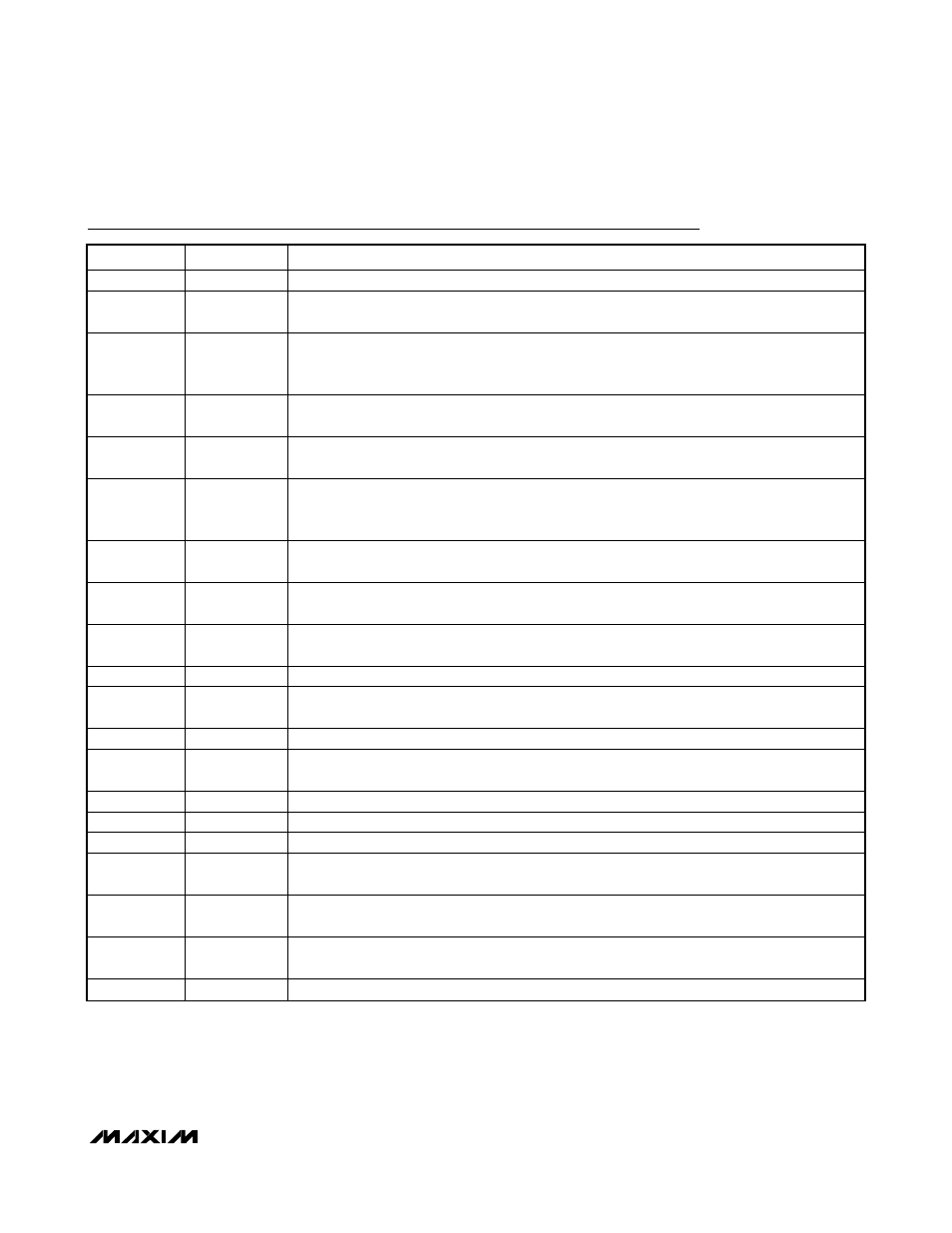
Pin Description
PIN
NAME
FUNCTION
1, 13, 37
GND
Input Buffer Supply and Digital Supply Ground
2
V
CCIN
Input Buffer Supply Voltage. Bypass to GND with 0.1µF and 0.001µF capacitors in parallel as
close to the device as possible, with the smallest value capacitor closest to the supply pin.
3–10,
39–48
RGB_IN[17:0]
LVTTL/LVCMOS Red, Green, and Blue Digital Video Data Inputs. Eighteen data bits are loaded
into the input latch on the rising edge of PCLK_IN when DE_IN is high. Internally pulled down to
GND.
11, 12, 15–21
CNTL_IN[8:0]
LVTTL/LVCMOS Control Data Inputs. Control data are latched on the rising edge of PCLK_IN
when DE_IN is low. Internally pulled down to GND.
14, 38
V
CC
Digital Supply Voltage. Bypass to GND with 0.1µF and 0.001µF capacitors in parallel as close to
the device as possible, with the smallest value capacitor closest to the supply pin.
22
DE_IN
LVTTL/LVCMOS Data Enable Input. Logic-high selects RGB_IN[17:0] to be latched. Logic-low
selects CNTL_IN[8:0] to be latched. DE_IN must be switching for proper operation. Internally
pulled down to GND.
23
PCLK_IN
LVTTL/LVCMOS Parallel Clock Input. Latches data and control inputs and provides the PLL
reference clock. Internally pulled down to GND.
24
MOD0
LVTTL/LVCMOS Modulation Rate Input. Selects the phase-modulation step size. Internally pulled
down to GND.
25
MOD1
LVTTL/LVCMOS Modulation Rate Input. Selects the phase-modulation step size. Internally pulled
down to GND.
26
PLL GND
PLL Supply Ground
27
V
CCPLL
PLL Supply Voltage. Bypass to PLL GND with 0.1µF and 0.001µF capacitors in parallel as close
to the device as possible, with the smallest value capacitor closest to the supply pin.
28
PWRDWN
LVTTL/LVCMOS Power-Down Input. Internally pulled down to GND.
29
CMF
Common-Mode Filter. Optionally connect a capacitor between CMF and ground to filter
common-mode switching noise.
30, 31
LVDS GND
LVDS Supply Ground
32
OUT-
Inverting LVDS Serial Data Output
33
OUT+
Noninverting LVDS Serial Data Output
34
V
CCLVDS
LVDS Supply Voltage. Bypass to LVDS GND with 0.1µF and 0.001µF capacitors in parallel as
close to the device as possible, with the smallest value capacitor closest to the supply pin.
35
RNG1
LVTTL/LVCMOS Frequency Range Select Input. Set to the frequency range that includes the
PCLK_IN frequency as shown in Table 3. Internally pulled down to GND.
36
RNG0
LVTTL/LVCMOS Frequency Range Select Input. Set to the frequency range that includes the
PCLK_IN frequency as shown in Table 3. Internally pulled down to GND.
EP
GND
Exposed Pad (Thin QFN Package Only). Connect Thin QFN exposed pad to PC board GND.