Dc electrical characteristics (continued) – Rainbow Electronics MAX9621 User Manual
Page 3
Dual, 2-Wire Hall-Effect Sensor Interface with
Analog and Digital Outputs
MAX9621
3
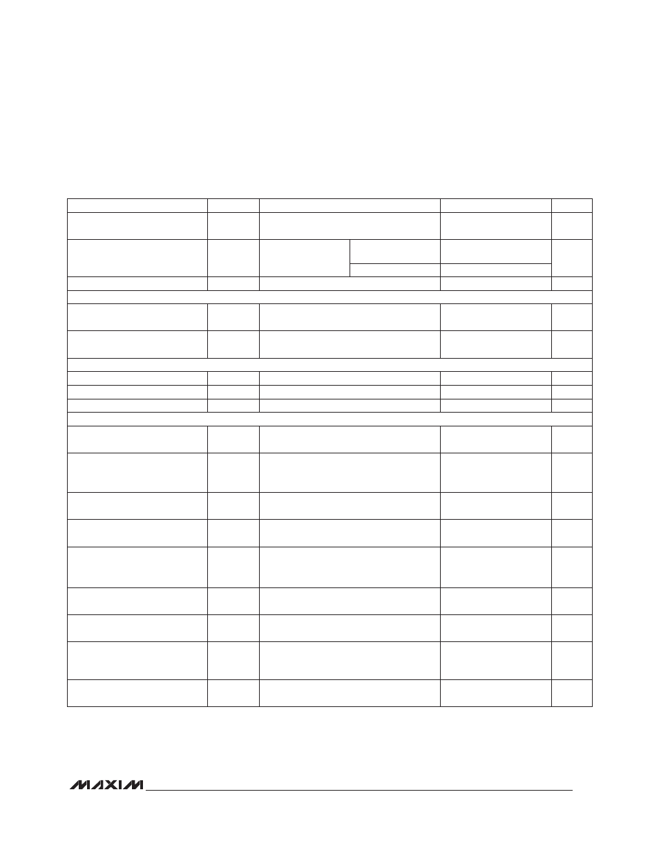
DC ELECTRICAL CHARACTERISTICS (continued)
(V
BAT
= 13.6V, V
SLEEP
= 5V, IN1 = IN2 = no connection, R
SET
= 61.9kI to BAT, R
PU
= 10kI at DOUT1 and DOUT2, R
L
= 5kI to
GND at AOUT1 and AOUT2, unless otherwise noted, T
A
= -40NC to +125NC. Typical values are at T
A
= +25NC.) (Note 1)
Note 1: All DC specifications are 100% production tested at T
A
= +25°C. AC specifications are guaranteed by design at T
A
=
+25°C.
Note 2: Parameters that change with the value of the R
SET
resistor: I
IH
, I
IL
, I
IN_HYS
, I
SC
, t
BL
, t
RAMP
, t
DEL
, f
MAX
, and P
R
.
Note 3: Following power-up or startup from sleep mode, the start of the blanking period is delayed 20Fs.
PARAMETER
SYMBOL
CONDITIONS
MIN
TYP
MAX
UNITS
Input Referred Current Offset
I
OS
Inferred from measurements at
I
IN
= -5mA, -14mA
-120
+120
F
A
AOUT_ Dropout Voltage
V
BAT
= 5.5V,
for 5% current
reduction
I
IN
= -14mA
0.85
1.6
V
I
IN
= -20mA
1.09
1.75
AOUT_ Output Impedance
500
MI
LOGIC I/O (DOUT1, DOUT2)
Output-Voltage Low DOUT1,
DOUT2
V
OL
Sink current = 1mA
0.4
V
Three-State Output Current
DOUT1, DOUT2
I
OZ
V
SLEEP
= 0V, 0V P V
DOUT_
P 5V
±1
F
A
SLEEP
Input-Voltage High
V
IH
2.0
V
Input-Voltage Low
V
IL
0.8
V
Input Resistance to GND
R
IN
50
100
kI
AC TIMING CHARACTERISTICS
Shutdown Delay from SLEEP
Low to IN_ Shutoff
t
SHDN
I
IH
= -14mA to GND, time from SLEEP low
to IN_ drop 500mV, C
L
= 20pF
33
40
46
F
s
IN_, Blanking Time at Hall
Sensor Power-Up
t
BL
I
IH
= -14mA to GND, time from
V
IN_
= 500mV until DOUT_ high, C
L
=
20pF (Notes 2, 3)
76
89
103
F
s
IN_, Current Ramp Rate After
Turn-On
t
RAMP
IN_ = GND (Note 2)
3.6
5
6.7
mA/Fs
Delay from IN_ to DOUT_ (Filter
Delay)
t
DEL
From I
IH
to I
IL
or from I
IL
to I
IH
,
C
L
= 20pF, Figure 1 (Note 2)
10.8
13.5
16
F
s
Delay Difference Between
Rising and Falling Edges of
Both Channels
t
DM
C
HALL-BYPASS
= 0.01FF, I
IH
= -11.5mA
and
I
IL
= -7.5mA, C
L
= 20pF
1
F
s
Delay Difference Between
Channels
t
CC
C
HALL-BYPASS
= 0.01FF, I
IH
= -11.5mA
and I
IL
= -7.5mA, C
L
= 20pF
500
ns
Maximum Frequency on Hall
Inputs
f
MAX
C
HALL-BYPASS
= 0.01FF, I
IH
= -11.5mA
and I
IL
= -7.5mA, C
L
= 20pF (Note 2)
34
39
kHz
Maximum Analog Output
Current During Short-to-GND
Fault
I
MAO
-1.4
mA
IN_ Pulse Length Rejected by
Filter to DOUT_
P
R
Figure 2 (Note 2)
7.8
11.5
14.6
F
s