Table 10. fan gain register (rfg/wfg), Table 11. fan full-scale register (rfs/wfs) – Rainbow Electronics MAX6660 User Manual
Page 16
MAX6660
Remote-Junction Temperature-Controlled
Fan-Speed Regulator with SMBus Interface
16
______________________________________________________________________________________
range of reference clock full-scale frequencies from
33Hz to 66Hz. A further division is performed to set the
actual desired fan speed. This value appears in the Fan-
Speed Control register in thermal closed-loop mode. If
the thermal loop is open, but the fan-speed control loop
is closed, this value is programmable in the fan DAC.
When in fan open-loop mode (which forces the thermal
loop to open), the FSC register becomes a true DAC,
programming the voltage across the fan from zero to
nearly 12V to V
VFAN
.
The tachometer input (TACH IN) includes a program-
mable (1/2/4/8) prescalar. The divider ratio for the
(1/2/4/8) prescalar is stored in the Fan Count Divisor
(FCD) register (Table 12). In general, the values in FC
should be set such that the full-speed fan frequency
divided by the prescalar fall in the 33Hz to 66Hz range.
The (UP/DN) counter has six stages that form the input
of a 6-bit resistive ladder DAC whose voltage is divided
down from V
VFAN
. This DAC determines the voltage
applied to the fan. Internal coding is structured such
that when in fan closed-loop mode (which includes
thermal closed loop) that higher values in the 0 to 32
range correspond to higher fan speeds and greater
voltage across the fan. In fan open-loop mode (which
forces thermal open loop) acceptable values range
from 0 to 63 (3Fh) for proportional control; a value of 64
(40h) commands unconditional full speed.
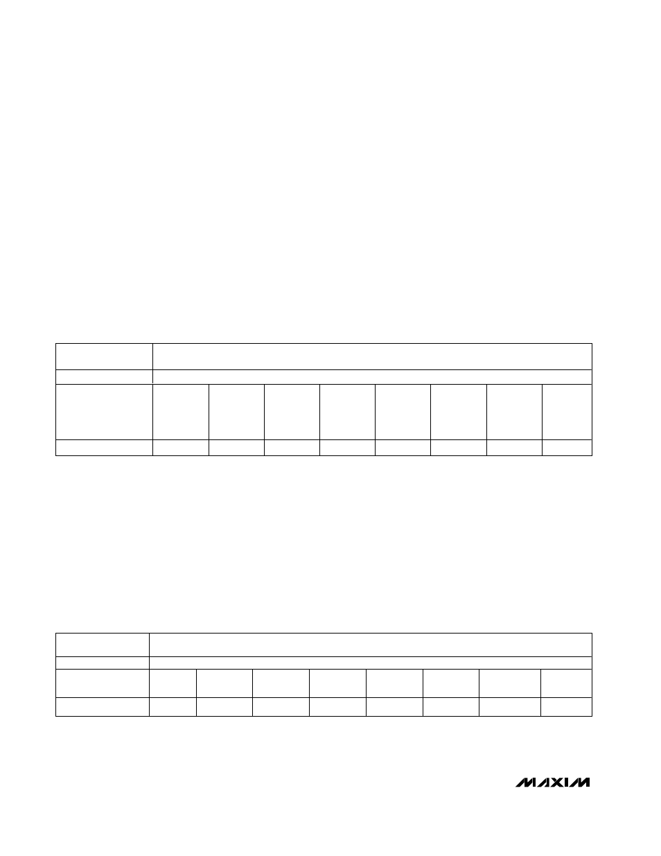
REGISTER/
ADDRESS
FG (16h = READ, 1Bh = WRITE)
COMMAND
READ/WRITE FAN GAIN REGISTER
Bit
7
Reserved
6
Fan Gain
5
Fan Gain
4
3
2
SMBus
Timeout
1
Fan
Feedback
Mode
0
Fan
Driver
Mode
POR State
1
0
0
x
x
x
0
0
Table 10. Fan Gain Register (RFG/WFG)
Notes:
Bit 7:
Reserved. Always 1. If bit 7 is written to zero, then bits 7, 6, and 5 are set to 100.
Bits 6, 5: Fan gain of the fan loop, where 00 = 8°C with resolution = 4 bits. This means that the fan reaches its full-scale (maximum)
speed when there is an 8°C difference between the remote-diode temperature and the value stored in TFAN
,
01 = 16°C,
with a 5-bit resolution and 10 = 32°C with a 6-bit resolution.
Bits 4, 3: Reserved.
Bit 2:
SMBus Timeout. When 1, the SMBus timeout is disabled. This permits full I
2
C compatibility with minimum clock frequency
to DC.
Bit 1:
Fan feedback mode. When bit 1 is set to 1, the fan loop uses driver current sense rather than tachometer feedback.
Bit 0:
Fan Driver Mode. When bit 0 is set to 1, the fan driver is in fan open-loop mode. In this mode, the fan DAC programs the
fan voltage rather than the fan speed. Tachometer feedback is ignored, and the user must consider minimum fan drive and
startup issues. Thermal open loop is automatically set to 1 (see Configuration register). Fan Fail (bit 0 of the Status register)
is set to 1 in this mode and should be ignored.
REGISTER/
ADDRESS
FS (1Fh = READ, 20h = WRITE)
COMMAND
READ/WRITE MAXIMUM TEMPERATURE LIMIT BYTE
Bit
7
(MSB)
6
Data Bit
5
Data Bit
4
Data Bit
3
Data Bit
2
Data Bit
1
Data Bit
0
Data Bit
POR State
1
1
1
1
1
1
1
1
Table 11. Fan Full-Scale Register (RFS/WFS)
Note: This register determines the maximum reference frequency at the input of the phase detector. It controls a programmable
divider that can be set anywhere between 127 and 255. The value in this register must be set in accordance with the proce-
dure described in the TACH IN section (equivalent to 8415/(Fan Frequency/Fan Count Divisor)). Programmed value below 127
defaults to 127. POR value is 255.