Applications information – Rainbow Electronics MAX6796 User Manual
Page 17

MAX6791–MAX6796
High-Voltage, Micropower, Single/Dual Linear
Regulators with Supervisory Functions
______________________________________________________________________________________
17
Applications Information
Output Voltage Selection
The MAX6791–MAX6796 feature dual-mode operation:
these devices operate in either a preset voltage mode
or an adjustable mode. In preset voltage mode, internal
trimmed feedback resistors set the internal linear regula-
tor to +1.8V, +2.5V, +3.3V, or +5V (see the Selector
Guide). Select preset voltage mode by connecting SET1
(MAX6791–MAX6794)/SET(MAX6795/MAX6796) to
GND. In adjustable mode, select an output voltage
between +1.8V and +11V using two external resistors
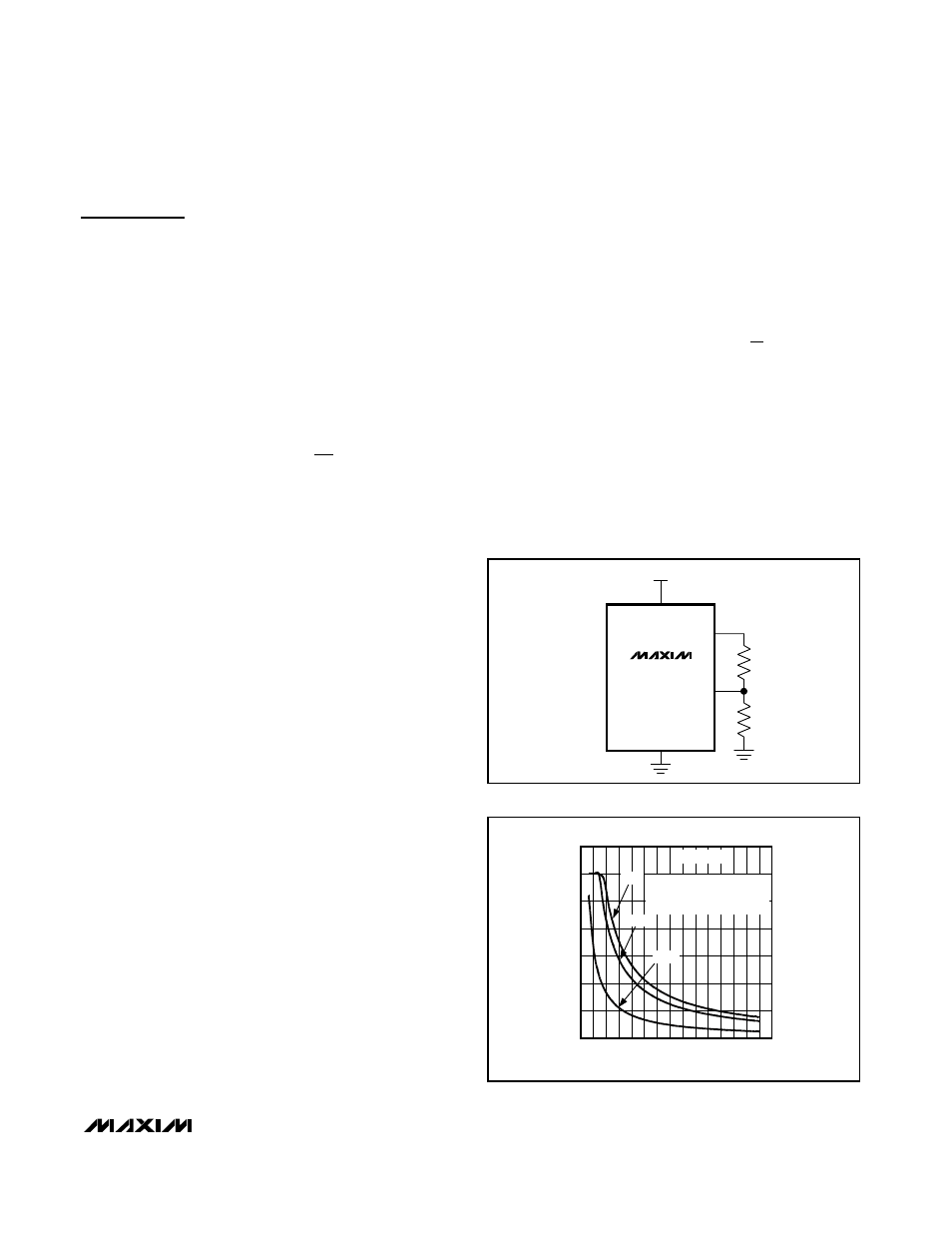
connected as a voltage-divider to SET1/SET (see Figure
1). Set the output voltage using the following equation:
where V
SET
= 1.2315V and R1, R2
≤ 200kΩ.
Available Output-Current Calculation
The MAX6791–MAX6794 provide up to 150mA per out-
put, and the MAX6795/MAX6796 provide up to 300mA
of load current. Since the input voltage can be as high
as +72V, package power dissipation limits the amount
of output current available for a given input/output volt-
age and ambient temperature. Figure 2 shows the max-
imum power-dissipation curve for the MAX6791–
MAX6796. The graph assumes that the exposed metal
pad of the device package is soldered to a solid 1in
2
section of PC board copper. Use Figure 2 to determine
the allowable package dissipation for a given ambient
temperature. Alternately, use the following formula to
calculate the allowable package dissipation:
PD
MAX
= Maximum Power Dissipation
PD
MAX
= 2.666W, for T
A
≤ +70°C
PD
MAX
= [2.666W - 0.0333W x (T
A
- 70°C)], for +70°C
< T
A
≤ +125°C
where 0.0333W is the MAX6791–MAX6796 package
thermal derating in W/°C and T
A
is the ambient temper-
ature in °C.
After determining the allowable package dissipation,
calculate the maximum output current using the follow-
ing formula:
PD = Power Dissipation
PD < PD
MAX
where PD = [(IN - OUT1) x I
OUT1
] + [(IN -
OUT2) x I
OUT2
], for MAX6791–MAX6794.
Also, I
OUT1
should be
≤ 150mA and I
OUT2
should be
≤ 150mA in any case.
PD < PD
MAX
where PD = [(IN - OUT) x I
OUT
], for
MAX6795/MAX6796.
Also, I
OUT
should be
≤ 300mA in any case.
Selecting Reset Timeout Period
The reset timeout period is adjustable to accommodate
a variety of µP applications. Adjust the reset timeout
period by connecting a capacitor between CSRT and
GND. Use the following formula to set the reset timeout
period:
where t
RP
is in seconds and C
CSRT
is in Farads.
Connect CSRT to OUT1 (MAX6791–MAX6794) or to
OUT (MAX6795/MAX6796) to select an internally fixed
timeout period. Connect CSRT to GND to force RESET
low. C
CSRT
must be a low-leakage (< 10nA) type
capacitor. Ceramic capacitors are recommended; do
not use capacitors lower than 100pF to avoid the influ-
ence of parasitic capacitances.
t
C
V
A
RP
CSRT
.
=
×
1 218
10
6
V
V
R
R
OUT
SET
=
+
1
1
2
MAX6791–MAX6796
V
IN
R1
R2
OUT1/OUT
SET1/SET
IN
GND
Figure 1. Setting the Output Voltage Using a Resistive-Divider
I
OUT
vs. (V
IN
- V
OUT
)
(V
IN
- V
OUT
) (V)
I
OUT
(mA)
70 75
60
50
40
30
20
10
50
100
150
200
250
300
350
0
0
+70
°C
+85
°C
+125
°C
V
OUT
= 1.8V
SAFE OPERATION REGION FOR
EACH TEMPERATURE POINT IS
UNDER THE CURVE
Figure 2. Maximum Power Dissipation for MAX6791–MAX6796
