Layout and power-supply bypassing – Rainbow Electronics MAX4029 User Manual
Page 10

MAX4028/MAX4029
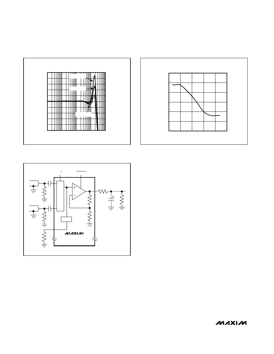
Although the MAX4028/MAX4029 are optimized for AC
performance and are not designed to drive highly
capacitive loads, they are capable of driving up to
15pF without oscillations. However, some peaking may
occur in the frequency domain (
Figure 4). To drive larg-
er capacitive loads or to reduce ringing, add an isola-
tion resistor between the amplifier’s output and the load
(Figure 5). The value of R
ISO
depends on the circuit’s
gain (+2V/V) and the capacitive load (Figure 6). Also
note that the isolation resistor forms a divider that
decreases the voltage delivered to the load.
Layout and Power-Supply Bypassing
The MAX4028/MAX4029 have high bandwidths and
consequently require careful board layout, including
the possible use of constant-impedance microstrip or
stripline techniques.
To realize the full AC performance of these high-speed
amplifiers, pay careful attention to power-supply
bypassing and board layout. The PC board should
have at least two layers: a signal and power layer on
one side, and a large, low-impedance ground plane on
the other side. The ground plane should be as free of
voids as possible. Whether or not a constant-imped-
ance board is used, it is best to observe the following
guidelines when designing the board:
1) Do not use wire-wrapped boards or breadboards.
2) Do not use IC sockets; they increase parasitic
capacitance and inductance.
3) Keep signal lines as short and straight as possible.
Do not make 90° turns; round all corners.
4) Observe high-frequency bypassing techniques to
maintain the amplifier’s accuracy and stability.
5) Use surface-mount components. They generally
have shorter bodies and lower parasitic reactance,
yielding better high-frequency performance than
through-hole components.
Triple/Quad, 2:1 Video
Multiplexer-Amplifiers with Input Clamps
10
______________________________________________________________________________________
SMALL-SIGNAL BANDWIDTH
vs. FREQUENCY
MAX4028 fig04
FREQUENCY (Hz)
SMALL-SIGNAL BANDWIDTH (dB)
100M
10M
1M
2
3
4
5
6
7
8
9
10
11
1
100k
1G
C
LOAD
= 15pF
C
LOAD
= 10pF
C
LOAD
= 5pF
Figure 4. Small-Signal Gain vs. Frequency with Capacitive
Load and No Isolation Resistor
R
ISO
R
L
C
L
R
T
75
Ω
OUT_
IN_A
IN_B
A/B
DISABLE
0.1
µF
75
Ω CABLE
R
T
75
Ω
0.1
µF
75
Ω CABLE
R
KEYREF
MAX4028
MAX4029
CLAMP
Figure 5. Using an Isolation Resistor (RISO) for a High-
Capacitive Load
OPTIMAL ISOLATION RESISTANCE
vs. CAPACITIVE LOAD
MAX4028 fig06
C
LOAD
(pF)
OPTIMAL ISOLATION RESISTANCE (
Ω)
200
150
100
50
5
10
15
20
25
30
0
0
250
Figure 6. Optimal Isolation Resistance vs. Capacitive Load
