Functional diagram – Rainbow Electronics MAX13047E User Manual
Page 9
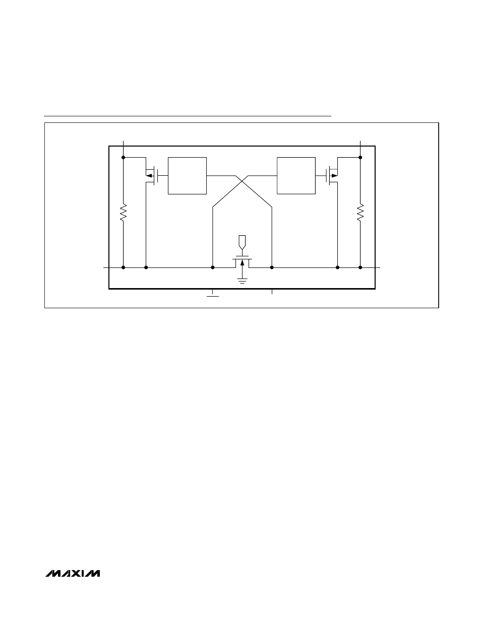
Level Translation
For proper operation, ensure that +1.65V ≤ V
CC
≤
+5.5V and +1.1V ≤ V
L
≤ the minimum of either +3.6V or
(V
CC
+ 0.3V). During power-up sequencing, V
L
≥ (V
CC
+ 0.3V) does not damage the device. The speed of the
rise time accelerator circuitry limits the maximum data
rate for the MAX13046E/MAX13047E to 16Mbps.
Rise-Time Accelerators
The MAX13046E/MAX13047E have an internal rise-time
accelerator, allowing operation up to 16Mbps. The rise-
time accelerators are present on both sides of the
device and act to speed up the rise time of the input
and output of the device, regardless of the direction of
the data. The triggering mechanism for these accelera-
tors is both level and edge sensitive. To guarantee
operation of the rise time accelerators the maximum
parasitic capacitance should be less than 200pF on the
I/O lines.
Shutdown Mode
Drive
SHDN low to place the MAX13046E/MAX13047E
in shutdown mode and drive
SHDN high for normal
operation. Activating the shutdown mode disconnects
the internal 10kΩ pullup resistors on the I/O V
CC
and I/O
V
L
lines. This forces the I/O lines to a high-impedance
state, and decreases the supply current to less than
1µA. The high-impedance I/O lines in shutdown mode
allow for use in a multidrop network. The MAX13046E/
MAX13047E have a diode from each I/O to the corre-
sponding supply rail and GND. Therefore, when in shut-
down mode, do not allow the voltage at I/O V
L
to
exceed (V
L
+ 0.3V), or the voltage at I/O V
CC
to exceed
(V
CC
+ 0.3V).
Operation with One Supply Disconnected
Certain applications require sections of circuitry to be
disconnected to save power. When V
L
is connected and
V
CC
is disconnected or connected to ground, the device
enters shutdown mode. In this mode, I/O V
L
can still be
driven without damage to the device; however, data
does not translate from I/O V
L
to I/O V
CC
. If V
CC
falls
more than V
TH_L_VCC
below V
L
, the device disconnects
the pullup resistors at I/O V
L
and I/O V
CC
. To achieve the
lowest possible supply current from V
L
when V
CC
is dis-
connected, it is recommended that the voltage at the
V
CC
supply input be approximately equal to GND.
When V
CC
is connected and V
L
is less than V
TH_VL
, the
device enters shutdown mode. In this mode, I/O V
CC
can still be driven without damage to the device; howev-
er, data does not translate from I/O V
CC
to I/O V
L
.
MAX13046E/MAX13047E
Single- and Dual-Bidirectional
Low-Level Translator
_______________________________________________________________________________________
9
ONE-SHOT
RISE-TIME
ACCELERATOR
V
L
SHDN
I/O V
L
I/O V
CC
V
CC
GATE BIAS
ONE-SHOT
RISE-TIME
ACCELERATOR
PU2
PU1
N
10k
Ω
10k
Ω
GND
Functional Diagram