Short-circuit protection, 15kv esd protection, Esd test conditions – Rainbow Electronics MAX13047E User Manual
Page 10: Human body model
MAX13046E/MAX13047E
When V
CC
is disconnected or connected to ground, I/O
V
CC
must not be driven more than V
CC
+ 0.3V. When V
L
is disconnected or connected to ground, I/O V
L
must
not be driven more than V
L
+ 0.3V.
Short-Circuit Protection
Thermal-overload detection protects the MAX13046E/
MAX13047E from short-circuit fault conditions. In the
event of a short-circuit fault, when the junction tempera-
ture (T
J
) exceeds +150°C, the device enters shutdown
mode. When the device has cooled to below +140°C,
normal operation resumes.
±15kV ESD Protection
ESD protection structures are incorporated on all pins
to protect against electrostatic discharges encountered
during handling and assembly. The ESD structures
withstand electrostatic discharge in all states: normal
operation, shutdown mode, and powered down. The
I/O V
CC
lines of the MAX13046E/MAX13047E are char-
acterized for protection to the following limit:
•
±15kV using the Human Body Model
ESD Test Conditions
ESD performance depends on a variety of conditions.
Contact Maxim for a reliability report that documents
test setup, test methodology, and test results.
Human Body Model
Figure 2a shows the Human Body Model, and Figure
2b shows the current waveform it generates when dis-
charged into a low-impedance state. This model con-
sists of a 100pF capacitor charged to the ESD voltage
of interest that is then discharged into the test device
through a 1.5kΩ resistor.
Single- and Dual-Bidirectional
Low-Level Translator
10
______________________________________________________________________________________
MAX13046E/
MAX13047E
I/O V
L
I/O V
CC
(t
RISE
,
t
FALL
< 10ns)
DATA
I/O V
CC
V
CC
V
CC
V
L
GND
R
L
C
L
t
PD-VCC-VL
t
PD-VCC-VL
I/O V
L
t
RVL
t
FVL
SHDN
V
L
R
S
50
Ω
MAX13046E/
MAX13047E
I/O V
L
I/O V
L
(t
RISE
,
t
FALL
< 10ns)
DATA
I/O V
CC
R
L
C
L
V
CC
V
CC
V
L
GND
t
PD-VL-VCC
t
PD-VL-VCC
I/O V
CC
t
RVCC
t
FVCC
SHDN
V
L
R
S
50
Ω
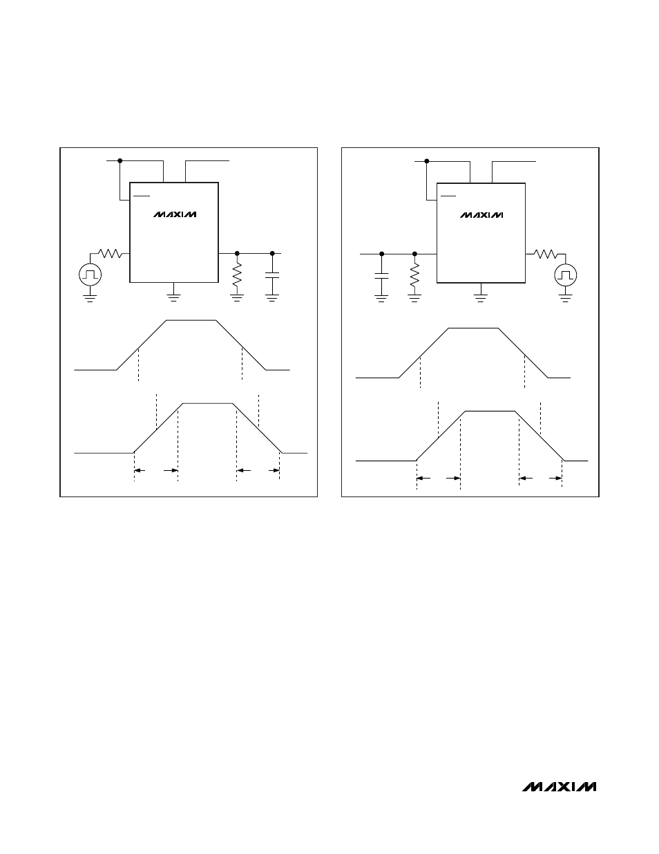
Figure 1a. Rail-to-Rail Driving I/O V
L
Figure 1b. Rail-to-Rail Driving I/O V
CC