Rainbow Electronics MAX13047E User Manual
Page 2
MAX13046E/MAX13047E
Single- and Dual-Bidirectional
Low-Level Translator
2
_______________________________________________________________________________________
ABSOLUTE MAXIMUM RATINGS
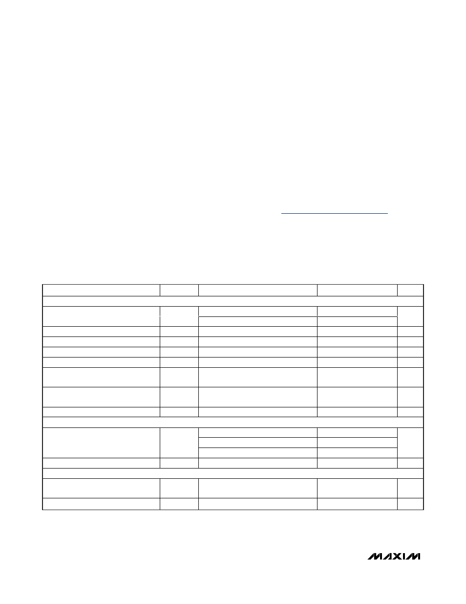
ELECTRICAL CHARACTERISTICS
(V
CC
= +1.65V to +5.5V, V
L
= +1.1V to minimum of either +3.6V or ((V
CC
+ 0.3V)), I/O V
L
and I/O V
CC
are unconnected, T
A
= -40°C to
+85°C, unless otherwise noted. Typical values are V
CC
= +3.3V, V
L
= +1.8V at T
A
= +25°C.) (Notes 2, 3)
Stresses beyond those listed under “Absolute Maximum Ratings” may cause permanent damage to the device. These are stress ratings only, and functional
operation of the device at these or any other conditions beyond those indicated in the operational sections of the specifications is not implied. Exposure to
absolute maximum rating conditions for extended periods may affect device reliability.
(All voltages referenced to GND.)
V
CC
...........................................................................-0.3V to +6V
V
L
..............................................................................-0.3V to +4V
I/O V
CC
.......................................................-0.3V to (V
CC
+ 0.3V)
I/O V
L
............................................................-0.3V to (V
L
+ 0.3V)
SHDN........................................................................-0.3V to +6V
Short-Circuit Duration I/O V
L
, I/O V
CC
to GND...........Continuous
Power Dissipation (T
A
= +70°C)
6-Pin µDFN (derate 2.1mW/°C above +70°C) .............168mW
10-Pin UTQFN (derate 6.9mW/°C above +70°C).........559mW
Junction-to-Ambient Thermal Resistance (
θ
JA
) (Note 1)
6-Pin µDFN .................................................................477°C/W
10-Pin UTQFN ...........................................................20.1°C/W
Junction-to-Ambient Thermal Resistance (
θ
JC
) (Note 1)
6-Pin µDFN ................................................................20.1°C/W
10-Pin UTQFN .........................................................143.1°C/W
Operating Temperature Range ...........................-40°C to +85°C
Junction Temperature ......................................................+150°C
Storage Temperature Range .............................-65°C to +150°C
Lead Temperature (soldering, 10s) .................................+300°C
PARAMETER
SYMBOL
CONDITIONS
MIN
TYP
MAX
UNITS
POWER SUPPLY
V
CC
> 3.3V
1.1
3.6V
V
L
Supply Range
V
L
V
CC
≤ 3.3V
1.1
V
CC
+ 0.3V
V
V
CC
Supply Range
V
CC
1.65
5.5
V
Supply Current from V
CC
I
QVCC
10
µA
Supply Current from V
L
I
QVL
15
µA
V
CC
Shutdown-Mode Supply Current
I
SD-VCC
T
A
= +25°C,
SHDN = GND
0.03
1
µA
V
L
Shutdown-Mode Supply Current
I
SD-VL
T
A
= +25°C,
SHDN = GND
0.03
1
µA
I/O V
L
and I/O V
CC
Shutdown-Mode
Leakage Current
I
SD-LKG
T
A
= +25°C,
SHDN = GND
0.02
0.5
µA
SHDN Input Leakage
T
A
= +25°C
0.02
0.1
µA
ESD PROTECTION
Human Body Model
±15V
IEC 61000-4-2 Air-Gap Discharge
±15V
I/O V
CC
(Note 4)
IEC 61000-4-2 Contact Discharge
±8V
kV
All Other Pins
Human Body Model
±2
kV
LOGIC-LEVEL THRESHOLDS
I/O V
L
Input-Voltage High
V
IHL
V
L
-
0.2
V
I/O V
L
Input-Voltage Low
V
ILL
0.15
V
Note 1: Package thermal resistances were obtained using the method described in JEDEC specification JESD51-7, using a four-layer
board. For detailed information on package thermal considerations, refer to
www.maxim-ic.com/thermal-tutorial
.