Rainbow Electronics MAX6696 User Manual
Page 15
byte’s POR state is 06h (4Hz). The MAX6695/MAX6696
use only the 3 LSBs of the control register. The 5 MSBs
are don’t care and should be set to zero. The conver-
sion rate tolerance is ±25% at any rate setting.
Valid A/D conversion results for all channels are avail-
able one total conversion time after initiating a conver-
sion, whether conversion is initiated through the
RUN/STOP bit, hardware STBY pin, one-shot com-
mand, or initial power-up.
Slave Addresses
The MAX6695 has a fixed address of 0011 000. The
MAX6696 device address can be set to any one of nine
different values at power-up by pin strapping ADD0
and ADD1 so that more than one MAX6695/MAX6696
can reside on the same bus without address conflicts
(Table 10).
The address pin states are checked at POR and RESET
only, and the address data stays latched to reduce qui-
escent supply current due to the bias current needed for
high-impedance state detection. The MAX6695/
MAX6696 also respond to the SMBus Alert Response
slave address (see the Alert Response Address section).
POR and UVLO
To prevent unreliable power-supply conditions from
corrupting the data in memory and causing erratic
behavior, a POR voltage detector monitors V
CC
and
clears the memory if V
CC
falls below 1.45V (typ; see
Electrical Characteristics). When power is first applied
and V
CC
rises above 2.0V (typ), the logic blocks begin
operating, although reads and writes at V
CC
levels
below 3.0V are not recommended.
Power-Up Defaults
• Interrupt latch is cleared.
• Address select pin is sampled.
• ADC begins autoconverting at a 4Hz rate for
channel 2/local and 8Hz for channel 1.
• Command register is set to 00h to facilitate quick
internal Receive Byte queries.
• T
HIGH
and T
LOW
registers are set to default max
and min limits, respectively.
• Hysteresis is set to 10
°C.
MAX6695/MAX6696
Dual Remote/Local Temperature Sensors with
SMBus Serial Interface
______________________________________________________________________________________
15
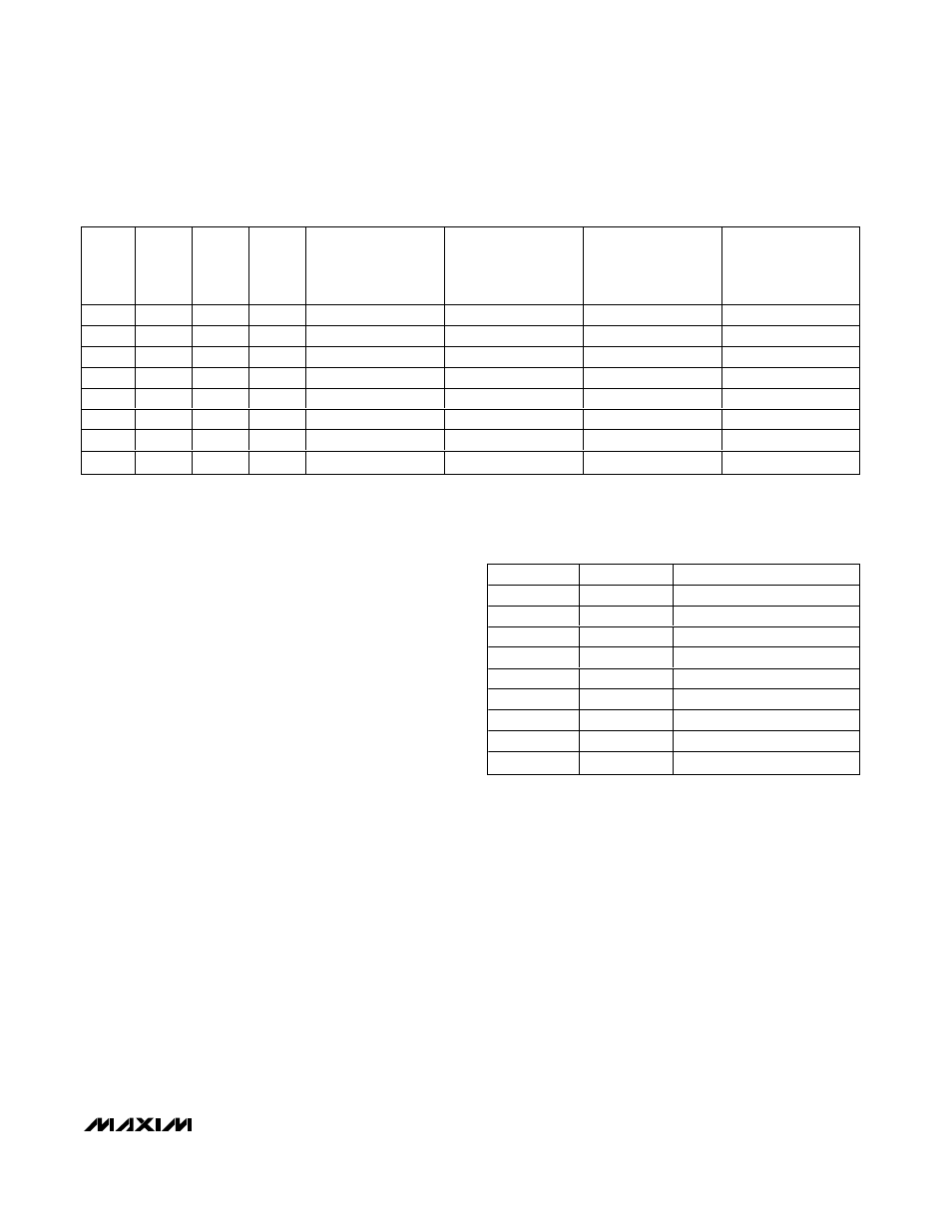
BIT 3
BIT 1
BIT0
HEX
CONVERSION
RATE (Hz) REMOTE
CHANNEL 2 AND
LOCAL
CONVERSION RATE
(Hz) REMOTE
CHANNEL 1
CONVERSION
PERIOD (s)
REMOTE CHANNEL
2 AND LOCAL
CONVERSION
PERIOD (s)
REMOTE CHANNEL
1
0
0
0
00h
0.0625
0.125
16
8
0
0
1
01h
0.125
0.25
8
4
0
1
0
02h
0.25
0.5
4
2
0
1
1
03h
0.5
1
2
1
1
0
0
04h
1
2
1
0.5
1
0
1
05h
2
4
0.5
0.25
1
1
0
06h
4
8
0.25
0.125
1
1
1
07h
4
8
0.25
0.125
Table 9. Conversion-Rate Control Register (POR = 0110)
ADD0
ADD1
ADDRESS
GND
GND
0011 000
GND
High-Z
0011 001
GND
V
CC
0011 010
High-Z
GND
0101 001
High-Z
High-Z
0101 010
High-Z
V
CC
0101 011
V
CC
GND
1001 100
V
CC
High-Z
1001 101
V
CC
V
CC
1001 110
Table 10. POR Slave Address Decoding
(ADD0 and ADD1)
Note:
Extended resolution applies only for conversion rate control register values of 05h or less.