Detailed description – Rainbow Electronics MAX6920 User Manual
Page 6

MAX6920
12-Output, 76V, Serial-Interfaced
VFD Tube Driver
6
_______________________________________________________________________________________
Detailed Description
The MAX6920 is a VFD tube driver comprising a 4-wire
serial interface driving 12 high-voltage Rail-to-Rail®
output ports. The driver is suitable for both static and
multiplexed displays.
The output ports feature high current-sourcing capabili-
ty to drive current into grids and anodes of static or
multiplex VFDs. The ports also have active current sink-
ing for fast discharge of capacitive display electrodes
in multiplexing applications.
The 4-wire serial interface comprises a 12-bit shift reg-
ister and a 12-bit transparent latch. The shift register is
written through a clock input CLK and a data input DIN
and the data propagates to a data output DOUT. The
data output allows multiple drivers to be cascaded and
operated together. The output latch is transparent to
the shift register outputs when LOAD is high, and latch-
es the current state on the falling edge of LOAD.
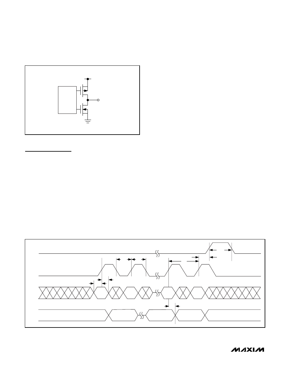
Each driver output is a slew-rated controlled CMOS
push-pull switch driving between V
BB
and GND. The
output rise time is always slower than the output fall
time to avoid shoot-through currents during output tran-
sitions. The output slew rates are slow enough to mini-
mize EMI, yet are fast enough so as not to impact the
typical 100µs digit multiplex period and affect the dis-
play intensity.
Initial Power-Up and Operation
An internal reset circuit clears the internal registers of
the MAX6920 on power-up. All outputs OUT0 to OUT11
and the interface output DOUT initialize low regardless
of the initial logic levels of the CLK, DIN, BLANK, and
LOAD inputs.
4-Wire Serial Interface
The MAX6920 uses a 4-wire serial interface with three
inputs (DIN, CLK, LOAD) and a data output (DOUT).
This interface is used to write output data to the
MAX6920 (
Figure
3) (
Table
1). The serial interface data
word length is 12 bits, D0–D11.
The functions of the four serial interface pins are:
•
CLK input is the interface clock, which shifts data
into the MAX6920’s 12-bit shift register on its rising
edge.
•
LOAD input passes data from the MAX6920’s 12-
bit shift register to the 12-bit output latch when
LOAD is high (transparent latch), and latches the
data on LOAD’s falling edge.
SLEW- RATE
CONTROL
V
BB
OUT_
40
Ω
TYPICAL
750
Ω
TYPICAL
Figure 2. MAX6920 CMOS Output Driver Structure
LOAD
t
CSW
t
CP
t
CSH
t
CH
t
DH
t
DO
t
DS
D11
D10
D1
D0
D11
t
CL
CLK
DIN
DOUT
Figure 3. 4-Wire Serial Interface Timing Diagram
Rail-to-Rail is a registered trademark of Nippon Motorola, Ltd.
