Electrical characteristics (continued) – Rainbow Electronics MAX6920 User Manual
Page 3
MAX6920
12-Output, 76V, Serial-Interfaced
VFD Tube Driver
_______________________________________________________________________________________
3
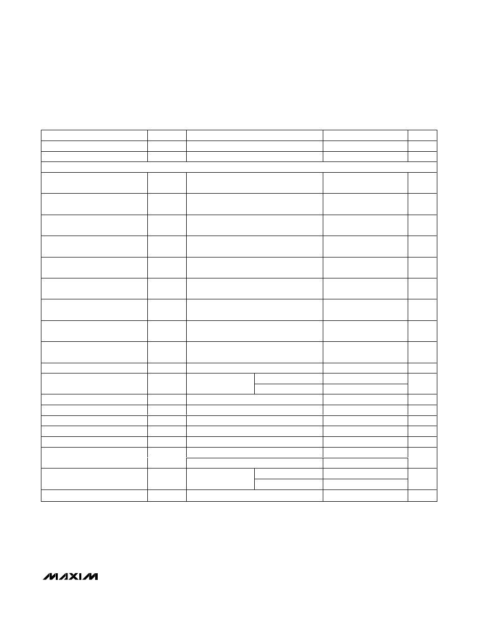
ELECTRICAL CHARACTERISTICS (continued)
(Typical Operating Circuit, V
BB
= 8V to 76V, V
CC
= 3V to 5.5V, T
A
= T
MIN
to T
MAX
, unless otherwise noted.) (Note 1)
PARAMETER
SYMBOL
CONDITIONS
MIN
TYP
MAX
UNITS
Rise Time OUT_ (20% to 80%)
t
R
V
BB
= 60V, C
L
= 50pF, R
L
= 2.3k
Ω
0.9
2
µs
Fall Time OUT_ (80% to 20%)
t
F
V
BB
= 60V, C
L
= 50pF, R
L
= 2.3k
Ω
0.6
1.5
µs
SERIAL INTERFACE TIMING CHARACTERISTICS
LOAD Rising to OUT_ Falling
Delay
(Notes 2, 3)
0.9
1.8
µs
LOAD Rising to OUT_ Rising
Delay
(Notes 2, 3)
1.2
2.4
µs
BLANK Rising to OUT_ Falling
Delay
(Notes 2, 3)
0.9
1.8
µs
BLANK Falling to OUT_ Rising
Delay
(Notes 2, 3)
1.3
2.5
µs
Input Leakage Current
CLK, DIN, LOAD, BLANK
I
IH
, I
IL
0.05
10
µA
Logic-High Input Voltage
CLK, DIN, LOAD, BLANK
V
IH
0.8 x
V
CC
V
Logic-Low Input Voltage
CLK, DIN, LOAD, BLANK
V
IL
0.3 x
V
CC
V
Hysteresis Voltage
DIN, CLK, LOAD, BLANK
∆V
I
0.6
V
High-Voltage DOUT
V
OH
I
SOURCE
= -1.0mA
V
CC
-
0.5
V
Low-Voltage DOUT
V
OL
I
SINK
= 1.0mA
0.5
V
3V to 4.5V
60
100
Rise and Fall Time DOUT
C
DOUT
= 10pF
(Note 2)
4.5V to 5.5V
30
80
ns
CLK Clock Period
t
CP
200
ns
CLK Pulse-Width High
t
CH
90
ns
CLK Pulse-Width Low
t
CL
90
ns
CLK Rise to LOAD Rise Hold
t
CSH
(Note 2)
100
ns
DIN Setup Time
t
DS
5
ns
3V to 4.5V
20
DIN Hold Time
t
DH
4.5V to 5.5V
15
ns
3.0V to 4.5V
25
120
240
DOUT Propagation Delay
t
DO
C
DOUT
= 10pF
4.5V to 5.5V
20
75
150
ns
LOAD Pulse High
t
CSW
55
ns
Note 1: All parameters are tested at T
A
= +25°C. Specifications over temperature are guaranteed by design.
Note 2: Guaranteed by design.
Note 3: Delay measured from control edge to when output OUT_ changes by 1V.