Rainbow Electronics MAX5735 User Manual
Page 9
MAX5732–MAX5735
32-Channel, 16-Bit, Voltage-Output
DACs with Serial Interface
_______________________________________________________________________________________
9
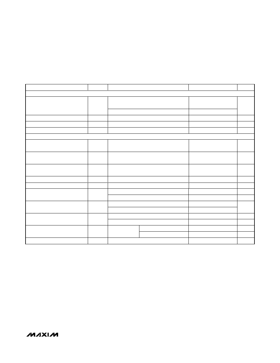
ELECTRICAL CHARACTERISTICS—MAX5735 (-5V to +5V Output Voltage Range) (continued)
(AV
CC
= +5.25V to +5.5V, AV
DD
= +5V ±5%, DV
DD
= +2.7V to AV
DD
, V
SS
= -5.25V to -5.5V, AGND = DGND = REFGND = GS = 0,
program the offset DAC to 8000hex. V
REF
= +3.0V, R
L
=
∞, C
L
= 50pF referenced to ground, T
A
= T
MIN
to T
MAX
, unless otherwise
noted. Typical values are at T
A
= +25°C.)
PARAMETER
SYMBOL
CONDITIONS
MIN
TYP
MAX
UNITS
DIGITAL INPUTS (
CS, SCLK, DIN, LDAC, CLR, DSP)
DV
DD
= +2.7V to +3.6V
0.7
×
DV
DD
Input-Voltage High
V
IH
DV
DD
= +4.75V to 5.25V
2.4
V
Input-Voltage Low
V
IL
0.8
V
Input Capacitance
C
IN
10
pF
Input Current
I
IN
Digital inputs = 0 or DV
DD
±1
µA
POWER REQUIREMENTS (AV
CC
, V
SS
, AGND, AV
DD
, DV
DD
, DGND)
Output-Amplifier Positive Supply
Voltage
AV
CC
4.75
5.50
V
Output-Amplifier Negative Supply
Voltage
V
SS
-5.50
-4.75
V
Output-Amplifier Supply Voltage
Difference
AV
CC
- V
SS
11
V
Analog Supply Voltage
AV
DD
4.75
5.25
V
Digital Supply Voltage
DV
DD
2.70
5.25
V
V
OUT0
through V
OUT31
= 0
10
15
mA
Analog Supply Current
AI
DD
Software shutdown
10
µA
V
IH
= DV
DD
, V
IL
= 0, f
SCLK
= 20MHz
2.5
3.5
Digital Supply Current
DI
DD
V
IH
= +2.4V, V
IL
= +0.8V, f
SCLK
= 20MHz
5
6.5
mA
V
OUT0
through V
OUT31
= 0
4
10
mA
Output-Amplifier Positive Supply
Current
AI
CC
Software shutdown
20
µA
V
OUT0
through V
OUT31
= 0
-4
-10
mA
Output-Amplifier Negative Supply
Current
I
SS
V
SS
= -0.5V
Software shutdown
-20
µA
Power-Supply Rejection Ratio
PSRR
-95
dB
Note 1: AV
CC
should be at least 0.25V higher than the maximum output voltage required from the DAC. Full-scale output is 5V for
the MAX5732.
Note 2: Linearity guaranteed from code 2047 to full scale and from (V
SS
+ 0.3V) to (AV
CC
- 0.3V).
Note 3: DNL guaranteed over all codes for (V
SS
+ 0.3V) to (AV
CC
- 0.3V).
Note 4: Zero-scale error is measured at code 0. Full-scale error is measured at code FFFFhex.
Note 5: DC crosstalk is the change in the output level of one DAC at midscale in response to the full-scale output change of all
other DACs.
Note 6: Digital feedthrough is a measure of the impulse injected into the analog outputs from the digital control inputs when the
device is not being written to. It is measured with a worst-case change on the digital inputs.
Note 7: Digital crosstalk is the glitch impulse transferred to the output of one DAC at midscale while a full-scale code change is written
into another DAC.
Note 8: DAC-to-DAC crosstalk is the glitch impulse that appears at the output of one converter due to both the digital change and
subsequent analog output change at another converter.