Rainbow Electronics MAX5735 User Manual
Page 2
MAX5732–MAX5735
32-Channel, 16-Bit, Voltage-Output
DACs with Serial Interface
2
_______________________________________________________________________________________
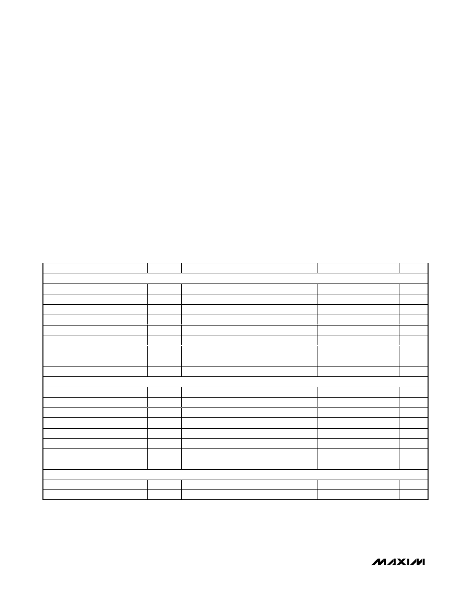
ABSOLUTE MAXIMUM RATINGS
ELECTRICAL CHARACTERISTICS—MAX5732 (0 to +5V Output Voltage Range)
(AV
CC
= +5.25V to +5.5V (Note 1), AV
DD
= +5V ±5%, DV
DD
= +2.7V to AV
DD
, V
SS
= AGND = DGND = REFGND = GS = 0, V
REF
=
+3.0V, R
L
=
∞, C
L
= 50pF referenced to ground, T
A
= T
MIN
to T
MAX
, unless otherwise noted. Typical values are at T
A
= +25°C.)
Stresses beyond those listed under “Absolute Maximum Ratings” may cause permanent damage to the device. These are stress ratings only, and functional
operation of the device at these or any other conditions beyond those indicated in the operational sections of the specifications is not implied. Exposure to
absolute maximum rating conditions for extended periods may affect device reliability.
AV
CC
to V
SS
, AGND, DGND, REFGND ..................-0.3V to +12V
V
SS
to AGND, DGND................................................-6V to +0.3V
AV
DD
, DV
DD
to AGND, DGND, REFGND.................-0.3V to +6V
AGND to DGND.....................................................-0.3V to +0.3V
REF to AGND, DGND,
REFGND...............-0.3V to the lower of (AV
DD
+ 0.3V) and +6V
REFGND to AGND.................................................-0.3V to +0.3V
Digital Inputs to AGND, DGND,
REFGND..............-0.3V to the lower of (DVDD + 0.3V) and +6V
DOUT to DGND.......-0.3V to the lower of (DV
DD
+ 0.3V) and +6V
OUT_ to V
SS
.........-0.3V to the lower of (AV
CC
+ 0.3V) and +12V
GS to AGND ................................................................-1V to +1V
Maximum Current into REF...............................................±10mA
Maximum Current into Any Pin .........................................±50mA
Continuous Power Dissipation (T
A
= +70°C)
Thin QFN (derate 31.3mW/°C above +70°C)...................2.5W
Operating Temperature Ranges
MAX573__CTN....................................................0°C to +70°C
MAX573__ETN .................................................-40°C to +85°C
Junction Temperature ......................................................+150°C
Storage Temperature Range .............................-65°C to +150°C
Lead Temperature (soldering, 10s) .................................+300°C
PARAMETER
SYMBOL
CONDITIONS
MIN
TYP
MAX
UNITS
DC CHARACTERISTICS
Resolution
N
16
Bits
Integral Nonlinearity
INL
MAX5732B (Note 2)
±8
±16
LSB
Differential Nonlinearity
DNL
Guaranteed monotonic (Note 3)
±1
LSB
Zero-Scale Error
V
OS
V
SS
= -0.5V, AV
CC
= +5.25V (Note 4)
±8
±40
mV
Full-Scale Error
(Note 4)
±8
±50
mV
Gain Error
±0.1
±0.5
%FSR
Gain Temperature Coefficient
20
40
ppm
FSR/°C
DC Crosstalk
V
SS
= -0.5V, AV
CC
= +5V (Note 5)
50
250
µV
DYNAMIC CHARACTERISTICS
Output-Voltage Settling Time
Full-scale change to ±0.5 LSB
20
µs
Voltage-Output Slew Rate
1
V/µs
Digital Feedthrough
(Note 6)
5
nV-s
Digital Crosstalk
(Note 7)
5
nV-s
Digital-to-Analog Glitch Impulse
Major carry transition
120
nV-s
DAC-to-DAC Crosstalk
(Note 8)
15
nV-s
Output Noise Spectral Density at
1kHz
Full-scale code
250
nV/
√Hz
ANALOG OUTPUTS (OUT0 to OUT31)
Output Voltage Range
V
SS
= -0.5V, AV
CC
= +5V
0
5
V
Resistive Load to Ground
10
50
k
Ω