Selector guide, Pin configuration, Chip information – Rainbow Electronics MAX5735 User Manual
Page 25: Power supplies, bypassing, decoupling, and layout
MAX5732–MAX5735
32-Channel, 16-Bit, Voltage-Output
DACs with Serial Interface
______________________________________________________________________________________
25
Selector Guide
PART
INL (MAX LSB)
OUTPUT VOLTAGE
RANGE (V)
MAX5732ACTN
±8
0 to +5
MAX5732BCTN
±16
0 to +5
MAX5732AETN
±8
0 to +5
MAX5732BETN
±16
0 to +5
MAX5733ACTN
±8
0 to +10
MAX5733BCTN
±16
0 to +10
MAX5733AETN
±8
0 to +10
MAX5733BETN
±16
0 to +10
MAX5734ACTN
±8
-2.5 to +7.5
MAX5734BCTN
±16
-2.5 to +7.5
MAX5734AETN
±8
-2.5 to +7.5
MAX5734BETN
±16
-2.5 to +7.5
MAX5735ACTN
±8
-5 to +5
MAX5735BCTN
±16
-5 to +5
MAX5735AETN
±8
-5 to +5
MAX5735BETN
±16
-5 to +5
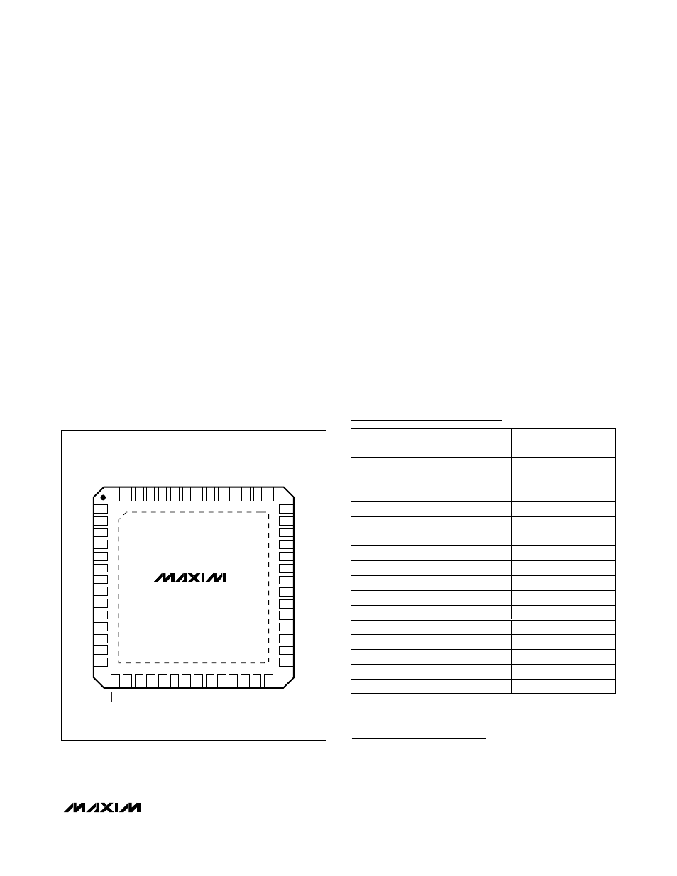
Pin Configuration
TOP VIEW
MAX5732
MAX5733
MAX5734
MAX5735
V
SS
OUT3
AGND
OUT4
OUT5
OUT6
OUT0
OUT1
OUT2
N.C.
OUT7
OUT8
OUT9
AV
CC
11
10
9
8
7
6
5
4
3
2
14
13
12
1
EXPOSED PADDLE
CS
8mm x 8mm THIN QFN-EP
DSP
SCLK
DOUT
DV
DD
DIN
LDAC
DGND
GS
CLR
REF
REFGND
V
SS
AV
DD
20
19
18
17
16
24
23
22
21
15
26
25
28
27
29
30
31
32
33
34
35
36
37
38
AGND
OUT23
OUT24
OUT25
OUT26
OUT27
OUT28
OUT29
OUT30
OUT31
39
V
SS
40
41
OUT21
OUT22
42
AV
CC
46
47
48
49
50
43
44
45
51
OUT15
AV
DD
REFGND
AV
CC
OUT16
OUT17
OUT18
OUT19
OUT20
52
OUT14
53
54
55
OUT11
OUT12
OUT13
56
OUT10
Chip Information
TRANSISTOR COUNT: 152,000
PROCESS: BiCMOS
Rail-to-Rail is a registered trademark of Nippon Motorola, Inc.
breakdown voltages. Some devices require external
protection on their reference inputs to satisfy absolute
maximum ratings. The MAX5734 features outputs that
are almost Rail-to-Rail
®
. This allows the AV
CC
and V
SS
supplies to be set to voltages within the absolute maxi-
mum ratings of the PEIC. This guarantees that the PEIC
is protected in all situations.
Additional protection is provided by the MAX5734
glitch-free power-up into the clear state with all DAC
outputs set to approximately 0V. Either the serial port or
the
CLR input can assert the clear function.
Power Supplies, Bypassing,
Decoupling, and Layout
Grounding and power-supply decoupling strongly influ-
ence device performance. Digital signals can couple
through the reference input, power supplies, and ground
connection. Proper grounding and layout can reduce
digital feedthrough and crosstalk. Bypass all power sup-
plies with an additional 0.1µF and 1µF on each pin, as
close to the device as possible. Refer to the MAX5732–
MAX5735 evaluation kit for a suggested layout.
The MAX5732–MAX5735 have four separate power
supplies. AV
DD
powers the internal analog circuitry
(except for the output buffers) and DV
DD
powers the
digital section of the device. AV
CC
and V
SS
power the
output buffers.
The MAX5732–MAX5735 feature an exposed paddle on
the backside of the package for improved power dissipa-
tion. The exposed paddle is electrically connected to
V
SS
, and should be soldered to a large copper plane that
shares the same potential. For more information on the
exposed paddle QFN package, refer to the following
website: http://pdfserv.maxim-ic.com/arpdf/AppNotes/
4hfan081.pdf