Rainbow Electronics MAX9770 User Manual
Page 2
MAX9770
1.2W Low-EMI, Filterless, Mono Class D Amplifier
with Stereo DirectDrive Headphone Amplifiers
2
_______________________________________________________________________________________
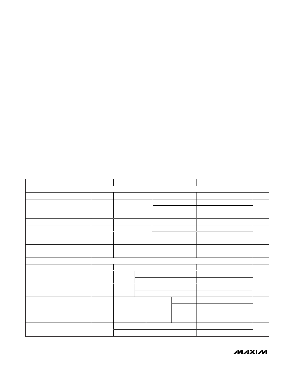
ABSOLUTE MAXIMUM RATINGS
ELECTRICAL CHARACTERISTICS
(V
DD
= PV
DD
= CPV
DD
= 3.3V, GND = PGND = CPGND = 0V,
SHDN = 3.3V, C1 = C2 = 1µF, C
BIAS
= 0.047µF, SYNC = GND, R
L
=
∞,
speaker load connected between OUT+ and OUT-, headphone load connected between HPOUT_ and GND, T
A
= T
MIN
to T
MAX
,
unless otherwise noted. Typical values are at T
A
= +25°C.) (Notes 1, 2)
Stresses beyond those listed under “Absolute Maximum Ratings” may cause permanent damage to the device. These are stress ratings only, and functional
operation of the device at these or any other conditions beyond those indicated in the operational sections of the specifications is not implied. Exposure to
absolute maximum rating conditions for extended periods may affect device reliability.
GND to PGND to CPGND......................................-0.3V to +0.3V
V
DD
to PV
DD
to CPV
DD
..........................................-0.3V to +0.3V
V
DD
to GND..............................................................................6V
PV
DD
to PGND .........................................................................6V
CPV
DD
to CPGND ....................................................................6V
CPV
SS
to CPGND....................................................................-6V
SV
SS
to GND ...........................................................................-6V
C1N..........................................(PV
SS
- 0.3V) to (CPGND + 0.3V)
HPOUT_ to GND ....................................................................
±3V
All other pins to GND..................................-0.3V to (V
DD
+ 0.3V)
Continuous Current Into/Out of:
PV
DD
, PGND, OUT_ ......................................................600mA
PV
SS
..............................................................................260mA
Duration of HPOUT_ Short Circuit to V
DD
, PV
DD
,
GND, PGND ...........................................................Continuous
Duration of Short Circuit between
HPOUTL and HPOUTR ..........................................Continuous
Duration of OUT_ Short Circuit to V
DD
, PV
DD
, GND, PGND ..10s
Duration of Short Circuit Between OUT+ and OUT-...............10s
Continuous Power Dissipation (T
A
= +70°C)
28-Pin TQFN (derate 20.8mW/°C above +70°C) .......1667mW
28-Pin TSSOP (derate 12.8mW°C above +70°C) ......1026mW
Junction Temperature ......................................................+150°C
Operating Temperature Range ...........................-40°C to +85°C
Storage Temperature Range .............................-65°C to +150°C
Lead Temperature (soldering, 10s) .................................+300°C
PARAMETER
SYMBOL
CONDITIONS
MIN
TYP
MAX
UNITS
GENERAL
Supply Voltage Range
V
DD
Inferred from PSRR test
2.5
5.5
V
Headphone mode
5.5
10
Quiescent Supply Current
I
DD
No load
Speaker mode
5.2
7.5
mA
Shutdown Supply Current
I
SHDN
SHDN = HPS = GND
0.1
10
µA
Shutdown to Full Operation
t
ON
50
ms
MONO
7
10
Input Impedance
R
IN
(Note 3)
INL_, INR_
14
20
k
Ω
Bias Voltage
V
BIAS
1.1
1.25
1.4
V
Feedthrough
From any unselected input to any output,
f = 10kHz
70
dB
SPEAKER AMPLIFIER (GAIN1 = GAIN2 = V
DD
, HPS = GND)
Output Offset Voltage
V
OS
±15
±70
mV
V
DD
= 2.5V to 5.5V
50
70
V
RIPPLE
= 200mV
P-P
, f = 217Hz
70
V
RIPPLE
= 200mV
P-P
, f = 1kHz
68
Power-Supply Rejection Ratio
PSRR
(Note 4)
V
RIPPLE
= 200mV
P-P
, f = 20kHz
50
dB
R
L
= 8
Ω
550
V
DD
= 3.3V
R
L
= 4
Ω
900
Output Power
P
OUT
f = 1kHz,
THD+N = 1%,
GAIN1 = 1,
GAIN2 = 0
V
DD
= 5V
R
L
= 8
Ω
1200
mW
R
L
= 8
Ω, P
OUT
= 300mW, f = 1kHz
0.025
Total Harmonic Distortion Plus
Noise
THD+N
R
L
= 4
Ω, P
OUT
= 300mW, f = 1kHz
0.03
%