Max9770, Table 5. suggested capacitor manufacturers – Rainbow Electronics MAX9770 User Manual
Page 18
MAX9770
Charge-Pump Capacitor Selection
Use capacitors with an ESR less than 100m
Ω for opti-
mum performance. Low-ESR ceramic capacitors mini-
mize the output resistance of the charge pump. Most
surface-mount ceramic capacitors satisfy the ESR
requirement. For best performance over the extended
temperature range, select capacitors with an X7R
dielectric. Table 5 lists suggested manufacturers.
Flying Capacitor (C1)
The value of the flying capacitor (C1) affects the load
regulation and output resistance of the charge pump. A
C1 value that is too small degrades the device’s ability to
provide sufficient current drive, which leads to a loss of
output voltage. Increasing the value of C1 may improve
load regulation and reduces the charge-pump output
resistance to an extent. Above 1µF, the on-resistance of
the switches and the ESR of C1 and C2 dominate.
Output Capacitor (C2)
The output capacitor value and ESR directly affect the
ripple at CPV
SS
. Increasing the value of C2 reduces
output ripple. Likewise, decreasing the ESR of C2
reduces both ripple and output resistance. Lower
capacitance values can be used in systems with low
maximum output power levels. See the Output Power
vs. Charge Pump Capacitance and Load Resistance
graph in the Typical Operating Characteristics.
CPV
DD
Bypass Capacitor
The CPV
DD
bypass capacitor (C3) lowers the output
impedance of the power supply and reduces the
impact of the MAX9770’s charge-pump switching tran-
sients. Bypass CPV
DD
with C3, the same value as C1,
and place it physically close to the CPV
DD
and PGND
(refer to the MAX9770 EV kit for a suggested layout).
Layout and Grounding
Proper layout and grounding are essential for optimum
performance. Use large traces for the power-supply
inputs and amplifier outputs to minimize losses due to
parasitic trace resistance, as well as route the head
away from the device. Good grounding improves audio
performance, minimizes crosstalk between channels,
and prevents any switching noise from coupling into
the audio signal. Connect CPGND, PGND, and GND
together at a single point on the PC board. Route
CPGND and all traces that carry switching transients
away from GND, PGND, and the traces and compo-
nents in the audio signal path.
Connect all components associated with the charge
pump (C2 and C3) to the CPGND plane. Connect SV
SS
and CPV
SS
together at the device. Place the charge-
pump capacitors (C1, C2, and C3) as close to the
device as possible. Bypass V
DD
and PV
DD
with a 1µF
capacitor to GND. Place the bypass capacitors as
close to the device as possible.
Use large, low-resistance output traces. As load imped-
ance decreases, the current drawn from the device out-
puts increase. At higher current, the resistance of the
output traces decrease the power delivered to the load.
Large output, supply, and GND traces also improve the
power dissipation of the device.
The MAX9770 thin QFN package features an exposed
thermal pad on its underside. This pad lowers the pack-
age’s thermal resistance by providing a direct heat con-
duction path. Due to the high efficiency of the MAX9770’s
Class D amplifier, additional heatsinking is not required. If
additional heatsinking is required, connect the exposed
paddle to GND. See the MAX9770 EV kit data sheet for
suggested component values and layout guidelines.
1.2W Low-EMI, Filterless, Mono Class D Amplifier
with Stereo DirectDrive Headphone Amplifiers
18
______________________________________________________________________________________
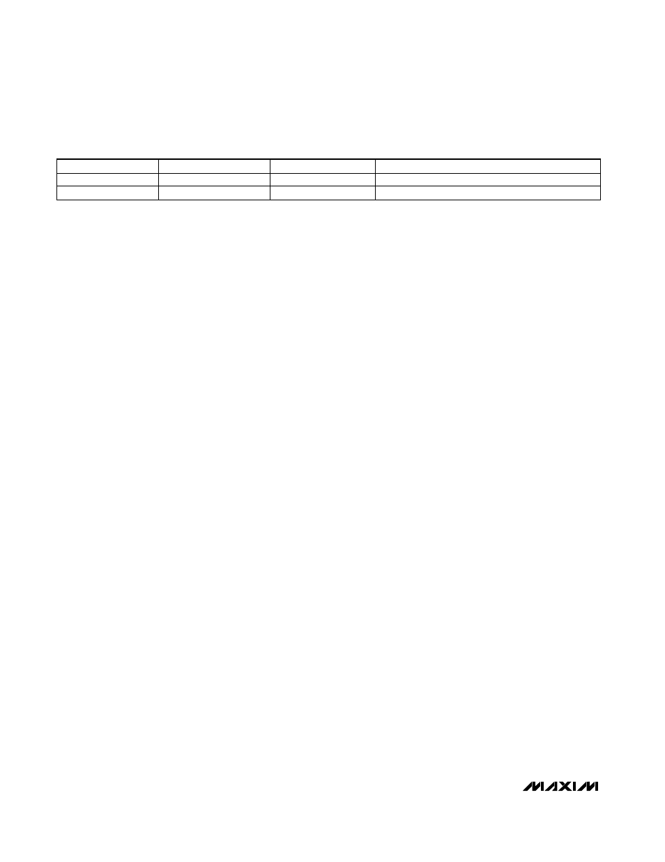
Table 5. Suggested Capacitor Manufacturers
SUPPLIER
PHONE
FAX
WEBSITE
Taiyo Yuden
800-348-2496
847-925-0899
www.t-yuden.com
TDK
807-803-6100
847-390-4405
www.component.tdk.com