Rainbow Electronics MAX13362 User Manual
Page 6
MAX13362
24-Channel Automotive Switch Monitor
6
_______________________________________________________________________________________
SWITCH THRESHOLD vs. VS VOLTAGE
(LOW-SIDE SWITCH)
MAX13362 toc10
VS VOLTAGE (V)
SWITCH THRESHOLD (V)
12
17
13
16
14
10
3.1
3.2
3.3
3.4
3.5
3.0
9
18
11
15
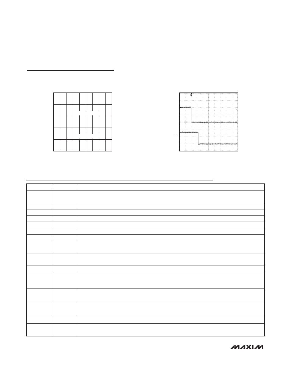
SWITCH OPEN TO CLOSE
SWITCH CLOSE TO OPEN
SWITCH STATUS CHANGE
(POLLING MODE)
MAX13362 toc11
2ms/div
V
IN
V
INT
5V/div
2V/div
0V
0V
10V
Pin Description
Typical Operating Characteristics (continued)
(V
DD
= V
SD
= 5V, V
VS
= 14V, T
A
= +25°C, unless otherwise noted.)
PIN
NAME
FUNCTION
1, 2, 11,
29, 30
N.C.
No Connection. Not internally connected.
3
IN17
Switch Monitor Input Channel 17. Connect IN17 to a ground-connected switch.
4
IN18
Switch Monitor Input Channel 18. Connect IN18 to a ground-connected switch.
5
IN19
Switch Monitor Input Channel 19. Connect IN19 to a ground-connected switch.
6
IN20
Switch Monitor Input Channel 20. Connect IN20 to a ground-connected switch.
7
IN21
Switch Monitor Input Channel 21. Connect IN21 to a ground-connected switch.
8
IN22
Switch Monitor Input Channel 22. Connect IN22 to a ground-connected switch.
9
IN23
Switch Monitor Input Channel 23. Connect IN23 to a battery-connected or ground-connected switch.
When used for a battery-connected switch, add a 100
Ω series protection resistor to the input.
10
INT
Inter r up t Outp ut.
INT i s an op en- d r ai n outp ut that asser ts l ow w hen one or m or e of the i np uts ( IN 0–IN 23)
chang e state and ar e enab l ed for i nter r up ts, or w hen the over tem p er atur e thr eshol d i s exceed ed .
12
CLK
SPI Serial Clock Input
13
SDO
SPI Serial Data Output. SPI data is output on SDO on the rising edges of CLK while
CS is held low.
SDO is high impedance when
CS is high. Connect SDO to a microcontroller data input or to a
succeeding device in a daisy chain.
14
CS
SPI Chip-Select Input. Drive
CS low to enable clocking of data into and out of the IC. SPI data is
latched into the device on the rising edge of
CS.
15
SDI
SPI Serial Data Input. SPI data is latched into the internal shift register on the falling edges of CLK
while
CS is held low. SDI has an internal 50k
Ω pulldown resistor. Connect SDI to the SDO of a
preceding device in a daisy chain or to the microcontroller data output.
16, 18
GND
Ground. Pins 16 and 18 must be connected to ground.
17
V
DD
Logic Supply Voltage. Connect V
DD
to a 3.3V or 5V logic supply. Bypass V
DD
to GND with at least a
0.1µF capacitor placed as close as possible to V
DD
.