Rainbow Electronics MAX5842 User Manual
Page 2
MAX5842
Quad, 12-Bit, Low-Power, 2-Wire, Serial
Voltage-Output DAC
2
_______________________________________________________________________________________
ABSOLUTE MAXIMUM RATINGS
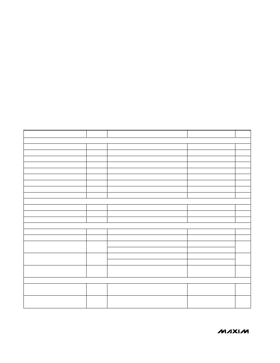
ELECTRICAL CHARACTERISTICS
(V
DD
= +2.7V to +5.5V, GND = 0, V
REF
= V
DD
, R
L
= 5k
Ω, C
L
= 200pF, T
A
= T
MIN
to T
MAX
, unless otherwise noted. Typical values are
at V
DD
= +5V, T
A
= +25°C.) (Note 1)
Stresses beyond those listed under “Absolute Maximum Ratings” may cause permanent damage to the device. These are stress ratings only, and functional
operation of the device at these or any other conditions beyond those indicated in the operational sections of the specifications is not implied. Exposure to
absolute maximum rating conditions for extended periods may affect device reliability.
V
DD
, SCL, SDA to GND ............................................-0.3V to +6V
OUT_, REF, ADD to GND..............................-0.3V to V
DD
+ 0.3V
Maximum Current into Any Pin............................................50mA
Continuous Power Dissipation (T
A
= +70°C)
10-Pin µMAX (derate 5.6mW above +70°C) .................444mW
Operating Temperature Range ...........................-40°C to +85°C
Storage Temperature Range .............................-65°C to +150°C
Maximum Junction Temperature .....................................+150°C
Lead Temperature (soldering, 10s) .................................+300°C
PARAMETER
SYMBOL
CONDITIONS
MIN
TYP
MAX
UNITS
STATIC ACCURACY (NOTE 2)
Resolution
N
12
Bits
Integral Nonlinearity
INL
(Note 3)
±2
±16
LSB
Differential Nonlinearity
DNL
Guaranteed monotonic (Note 3)
±1
LSB
Zero-Code Error
ZCE
Code = 000 hex, V
DD
= 2.7V
6
40
mV
Zero-Code Error Tempco
2.3
ppm/
o
C
Gain Error
GE
Code = FFF hex
-0.8
-3
%FSR
Gain-Error Tempco
0.26
ppm/
o
C
Power-Supply Rejection Ratio
PSRR
Code = FFF hex, V
DD
= 4.5V to 5.5V
58.8
dB
DC Crosstalk
30
µV
REFERENCE INPUT
Reference Input Voltage Range
V
REF
0
V
DD
V
Reference Input Impedance
32
45
k
Ω
Reference Current
Power-down mode
±0.3
±1
µA
DAC OUTPUT
Output Voltage Range
No load (Note 4)
0
V
DD
V
DC Output Impedance
Code = 800 hex
1.2
Ω
V
DD
= 5V, V
OUT
= full scale (short to GND)
42.2
Short-Circuit Current
V
DD
= 3V, V
OUT
= full scale (short to GND)
15.1
mA
V
DD
= 5V
8
Wake-Up Time
V
DD
= 3V
8
µs
DAC Output Leakage Current
Power-down mode = high impedance,
V
DD
= 5.5V, V
OUT
_ = V
DD
or GND
±0.1
±1
µA
DIGITAL INPUTS (SCL, SDA)
Input High Voltage
V
IH
0.7
✕
V
DD
V
Input Low Voltage
V
IL
0.3
✕
V
DD
V