C slave addresses – Rainbow Electronics MAX5842 User Manual
Page 10
MAX5842
Quad, 12-Bit, Low-Power, 2-Wire, Serial
Voltage-Output DAC
10
______________________________________________________________________________________
read operations require S
r
conditions because of the
change in direction of data flow.
Acknowledge Bit (ACK)
The acknowledge bit (ACK) is the ninth bit attached to
any 8-bit data word. ACK is always generated by the
receiving device. The MAX5842 generates an ACK
when receiving an address or data by pulling SDA low
during the ninth clock period. When transmitting data,
the MAX5842 waits for the receiving device to generate
an ACK. Monitoring ACK allows for detection of unsuc-
cessful data transfers. An unsuccessful data transfer
occurs if a receiving device is busy or if a system fault
has occurred. In the event of an unsuccessful data
transfer, the bus master should reattempt communica-
tion at a later time.
Slave Address
A bus master initiates communication with a slave
device by issuing a START condition followed by the
7-bit slave address (Figure 4). When idle, the MAX5842
waits for a START condition followed by its slave
address. The serial interface compares each address
value bit by bit, allowing the interface to power down
immediately if an incorrect address is detected. The
LSB of the address word is the Read/Write (R/W) bit.
R/W indicates whether the master is writing to or read-
ing from the MAX5842 (R/W = 0 selects the write condi-
tion, R/W = 1 selects the read condition). After
receiving the proper address, the MAX5842 issues an
ACK by pulling SDA low for one clock cycle.
The MAX5842 has four different factory/user-pro-
grammed addresses (Table 2). Address bits A6
through A1 are preset, while A0 is controlled by ADD.
Connecting ADD to GND sets A0 = 0. Connecting ADD
to V
DD
sets A0 = 1. This feature allows up to four
MAX5842s to share the same bus.
Write Data Format
In write mode (R/W = 0), data that follows the address
byte controls the MAX5842 (Figure 5). Bits C3-C0 con-
figure the MAX5842 (Table 3). Bits D11-D0 are DAC
data. Input and DAC registers update on the falling
edge of SCL during the acknowledge bit. Should the
write cycle be prematurely aborted, data is not updated
and the write cycle must be repeated. Figure 6 shows
two example write data sequences.
Extended Command Mode
The MAX5842 features an extended command mode
that is accessed by setting C3-C0 = 1 and D11-D8 = 0.
The next data byte writes to the shutdown registers
(Figure 7). Setting bits A, B, C, or D to 1 sets that DAC
SCL
SDA
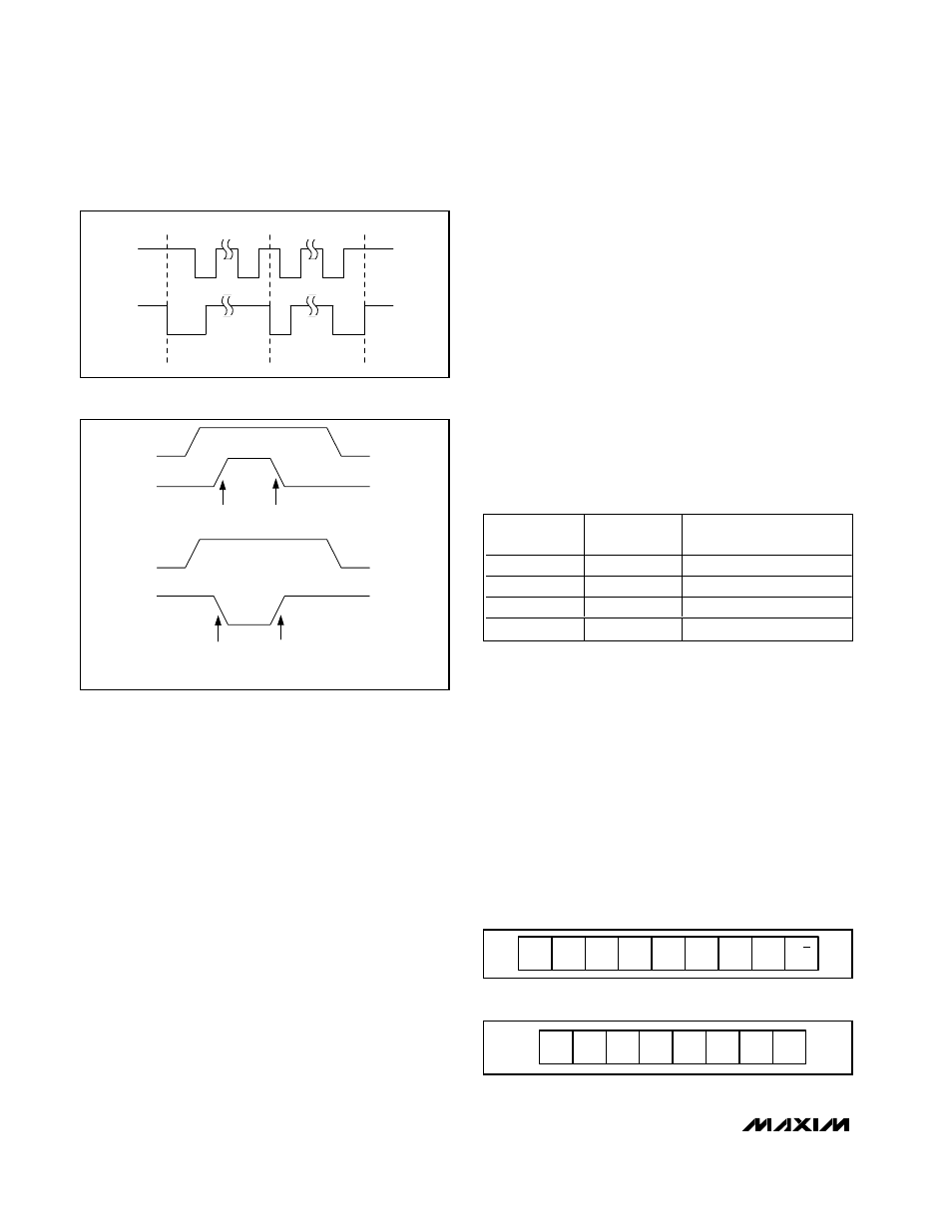
S
S
r
P
Figure 2. START and STOP Conditions
SCL
SDA
STOP
START
SCL
SDA
ILLEGAL
STOP
START
ILLEGAL EARLY STOP CONDITION
LEGAL STOP CONDITION
Figure 3. Early STOP Conditions
S
A6
A5
A4
A3
A2
A1
A0
R/W
Figure 4. Slave Address Byte Definition
C3
C2
C1
C0
D11
D10
D9
D8
Figure 5. Command Byte Definition
PART
V
ADD
DEVICE ADDRESS
(A6...A0)
MAX5842L
GND
0111 100
MAX5842L
V
DD
0111 101
MAX5842M
GND
1011 100
MAX5842M
V
DD
1011 101
Table 2. MAX5842 I
2
C Slave Addresses