Output, 76v, serial-interfaced vfd tube drivers, Table 1. 4-wire serial interface truth table – Rainbow Electronics MAX6931 User Manual
Page 8
MAX6921/MAX6931
Writing Device Registers Using the
4-Wire Serial Interface
The MAX6921/MAX6931 are normally written using the
following sequence:
1) Take CLK low.
2) Clock 20 bits of data in order D19 first to D0 last
into DIN, observing the data setup and hold times.
3) Load the 20 output latches with a falling edge
on LOAD.
LOAD may be high or low during a transmission. If
LOAD is high, then the data shifted into the shift regis-
ter at DIN appear at the OUT0 to OUT19 outputs.
CLK and DIN may be used to transmit data to other
peripherals. Activity on CLK always shifts data into the
MAX6921/MAX6931s’ shift register. However, the
MAX6921/MAX6931 only update their output latch on
the rising edge of LOAD, and the last 20 bits of data
are loaded. Therefore, multiple devices can share CLK
and DIN, as long as they have unique LOAD controls.
Determining Driver Output Voltage Drop
The outputs are CMOS drivers, and have a resistive
characteristic. The typical and maximum sink and
source output resistances can be calculated from the
V
H
and V
L
electrical characteristics. Use this calculated
resistance to determine the output voltage drop at dif-
ferent output currents.
20-Output, 76V, Serial-Interfaced
VFD Tube Drivers
8
_______________________________________________________________________________________
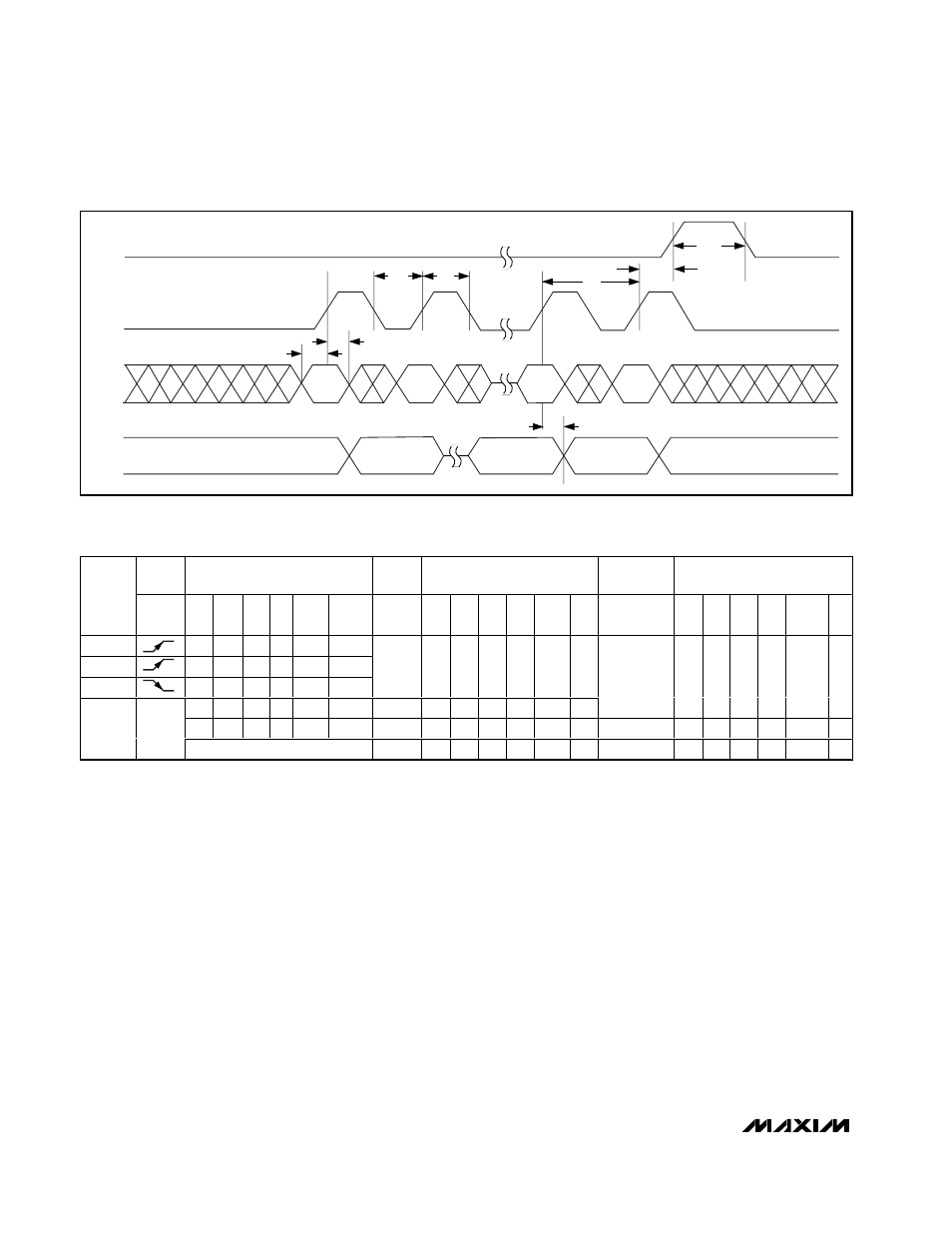
LOAD
t
CSW
t
CP
t
CSH
t
CH
t
DH
t
DO
t
DS
D19
D18
D1
D0
D19
t
CL
CLK
DIN
DOUT
Figure 4. 4-Wire Serial Interface Timing Diagram
CLOCK
INPUT
SHIFT REGISTER CONTENTS
LOAD
INPUT
LATCH CONTENTS
BLANKING
INPUT
OUTPUT CONTENTS
SERIAL
DATA
INPUT
DIN
CLK
D0
D1
D2 … Dn-1
Dn
LOAD
D0 D1
D2
… Dn-1 Dn
BLANK
D0 D1 D2
…
Dn-1 Dn
H
H
R0
R1 … Rn-2
Rn-1
L
L
R0
R1 … Rn-2
Rn-1
X
R0
R1
R2 … Rn-1
Rn
X
X
X
…
X
X
L
R0
R1
R2
…
Rn-1 Rn
P0
P1
P2 … Pn-1
Pn
H
P0
P1
P2
…
Pn-1 Pn
L
P0
P1
P2
…
Pn-1
Pn
X
X
X
…
X
X
H
L
L
L
…
L
L
Table 1. 4-Wire Serial Interface Truth Table
L = Low logic level.
H = High logic level.
X = Don’t care.
P = Present state (shift register).
R = Previous state (latched).