Pin description – Rainbow Electronics MAX6931 User Manual
Page 6
MAX6921/MAX6931
20-Output, 76V, Serial-Interfaced
VFD Tube Drivers
6
_______________________________________________________________________________________
PIN
TSSOP
MAX6931
MAX6921
WIDE SO/
PLCC
NAME
FUNCTION
1–5, 10–19,
24–28
—
—
OUT0 to
OUT19
VFD Anode and Grid Drivers. OUT0 to OUT19 are push-pull outputs swinging
from V
BB
to V
SS
.
—
1–5, 10–19,
24–28
3–12,
17–26
OUT0 to
OUT19
VFD Anode and Grid Drivers. OUT0 to OUT19 are push-pull outputs swinging
from V
BB
to GND.
—
9
2
DOUT
Serial-Clock Output. Data is clocked out of the internal shift-register to DOUT
on CLK’s rising edge.
6
6
27
DIN
Serial-Data Input. Data is loaded into the internal shift register on CLK’s rising
edge.
7
7
28
V
CC
Logic Supply Voltage
8
8
1
V
BB
VFD Tube Supply Voltage
9
—
—
V
SS
Filament Bias Supply Voltage
20
20
13
BLANK
Blanking Input. High forces outputs OUT0 to OUT19 low, without altering the
contents of the output latches. Low enables outputs OUT0 to OUT19 to follow
the state of the output latches.
21
21
14
GND
Ground
22
22
15
CLK
Serial-Clock Input. Data is loaded into the internal shift register on CLK’s
rising edge.
23
23
16
LOAD
Load Input. Data is loaded transparently from the internal shift register to the
output latch while LOAD is high. Data is latched into the output latch on
LOAD's rising edge, and retained while LOAD is low.
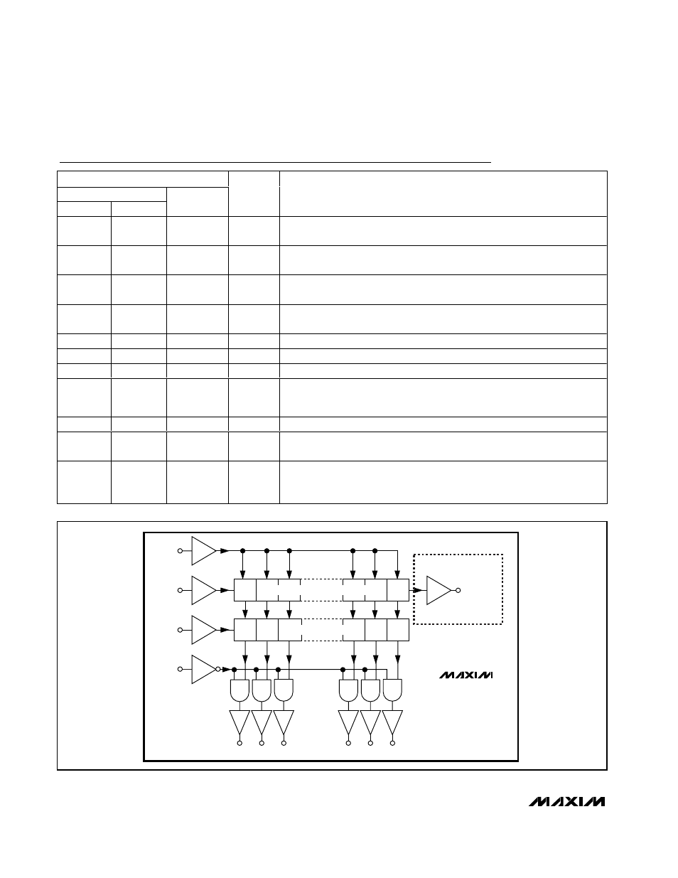
Pin Description
SERIAL-TO-PARALLEL SHIFT REGISTER
LATCHES
CLK
DIN
LOAD
BLANK
OUT0 OUT1 OUT2
OUT19
DOUT
MAX6921 ONLY
MAX6921
MAX6931
Figure 1. MAX6921/MAX6931 Functional Diagram