Rainbow Electronics MAX8620 User Manual
Page 9
Voltage-Positioning Load Regulation
As seen in
Figure 2, the MAX8620Y uses a unique step-
down converter feedback network. By taking feedback
from the LX node through R1, the usual phase lag due
to the output capacitor is removed, making the loop
exceedingly stable and allowing the use of a very small
ceramic output capacitor. This configuration causes the
output voltage to shift by the inductor series resistance
multiplied by the load current. This output-voltage shift
is known as voltage-positioning load regulation.
Voltage-positioning load regulation greatly reduces
overshoot during load transients, which effectively
halves the peak-to-peak output-voltage excursions
compared to traditional step-down converters. See the
Load-Transient Response graph in the Typical
Operating Characteristics section.
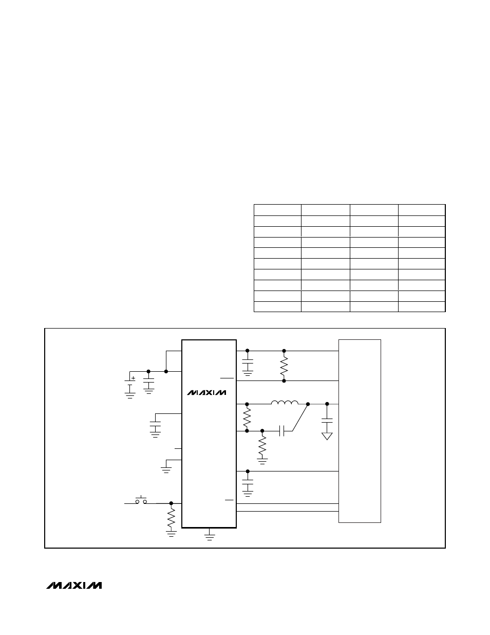
Two low-dropout, low-quiescent-current, high-accuracy
linear regulators supply loads up to 300mA each. The
LDO output voltages are set using SEL1 and SEL2 (see
Table 1). As shown in Figure 3, the LDOs include an
internal reference, error amplifiers, p-channel pass tran-
sistors, internal-programmable voltage-dividers, and an
OUT1 power-good comparator. Each error amplifier
compares the reference voltage to a feedback voltage
and amplifies the difference. If the feedback voltage is
lower than the reference voltage, the pass-transistor
gate is pulled lower, allowing more current to pass to
the outputs and increasing the output voltage. If the
feedback voltage is too high, the pass-transistor gate is
pulled up, allowing less current to pass to the output.
MAX8620Y
µPMIC for Microprocessors or DSPs
in Portable Equipment
_______________________________________________________________________________________
9
OUT1
OUT2
LX
FB
GND
IN1
BP
HF_PWR
2.6V
300mA
100k
Ω
PWR_ON
SEL1
RESET
SEL2
EN2
RESET IN
OUT3,
500mA
C
OUT2
4.7
µF
C
OUT1
4.7
µF
C
OUT3
2.2
µF
C
IN
10
µF
C
BP
0.01
µF
C
FF
150pF
DSP
OR
µP
I/O
ANALOG
ON/OFF
CORE
R1
150k
Ω
L
2.2
µH
Li+
CELL
2.6V
300mA
R2
75k
Ω
POWER-ON
KEY
V
BATT
1M
Ω
IN2
MAX8620Y
SEL1
SEL2
OUT1
OUT2
IN1
IN1
3.00V
2.50V
IN1
OPEN
2.85V
2.85V
IN1
GND
3.00V
3.00V
OPEN
IN1
3.30V
2.50V
OPEN
OPEN
2.80V
2.60V
OPEN
GND
3.30V
1.80V
GND
IN1
2.85V
2.60V
GND
OPEN
2.60V
2.60V
GND
GND
1.80V
2.60V
Figure 2. Typical MAX8620Y DSP or µP Application
Table 1. MAX8620Y Output-Voltage
Selection