Detailed description – Rainbow Electronics MAX8620 User Manual
Page 8

MAX8620Y
µPMIC for Microprocessors or DSPs
in Portable Equipment
8
_______________________________________________________________________________________
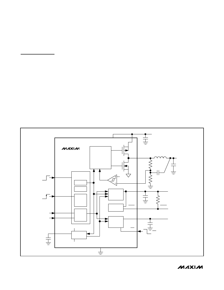
Detailed Description
The MAX8620Y µPMIC is designed to power low-core-
voltage microprocessors or DSPs in portable devices.
The µPMIC contains a fixed-frequency, high-efficiency
step-down converter; two low-dropout regulators
(LDOs); a 30ms (min) reset timer; and power-on/off
control logic (Figure 1).
Step-Down DC-DC Control Scheme
The MAX8620Y step-down converter is optimized for
high-efficiency voltage conversion over a wide load
range while maintaining excellent transient response,
minimizing external component size, and minimizing
output voltage ripple. The DC-DC converter (OUT3)
also features an optimized on-resistance internal
MOSFET switch and synchronous rectifier to maximize
efficiency. The MAX8620Y utilizes a proprietary hys-
teretic-PWM control scheme that switches with nearly
fixed frequency up to 4MHz, allowing for ultra-small
external components. The step-down converter output
current is guaranteed up to 500mA.
When the step-down converter output voltage falls
below the regulation threshold, the error comparator
begins a switching cycle by turning the high-side pFET
switch on. This switch remains on until the minimum on-
time (t
ON
) expires and the output voltage is in regula-
tion or the current-limit threshold (I
LIM3P
) is exceeded.
Once off, the high-side switch remains off until the mini-
mum off-time (t
OFF
) expires and the output voltage
again falls below the regulation threshold. During this
off period, the low-side synchronous rectifier turns on
and remains on until either the high-side switch turns
on or the inductor current reduces to the rectifier-off
current threshold (I
LXOFF
= 30mA (typ)). The internal
synchronous rectifier eliminates the need for an exter-
nal Schottky diode.
FB
LX
0.6V
STEP-DOWN
CONVERTER
CONTROL
pFET
nFET
LDO1
CONTROL
LDO2
CONTROL
OUT1
OUT2
REFERENCE
IN1
GND
OUTPUT-
VOLTAGE
SELECT
UVLO
CONTROL
LOGIC
ONE-
SHOT
TIMER
PWR_ON
HF_PWR
SEL1
SEL2
RESET
EN2
BP
RESET
ENABLE
R1
R2
L
V
IN
C
IN
C
OUT3
C
OUT1
R
PU
C
BP
C
OUT2
C
FF
OUT3
GND
OUT1
OUT2
EN2
RESET
IN2
IN1
MAX8620Y
Figure 1. Functional Diagram
