Pin description – Rainbow Electronics MAX8620 User Manual
Page 7
MAX8620Y
µPMIC for Microprocessors or DSPs
in Portable Equipment
_______________________________________________________________________________________
7
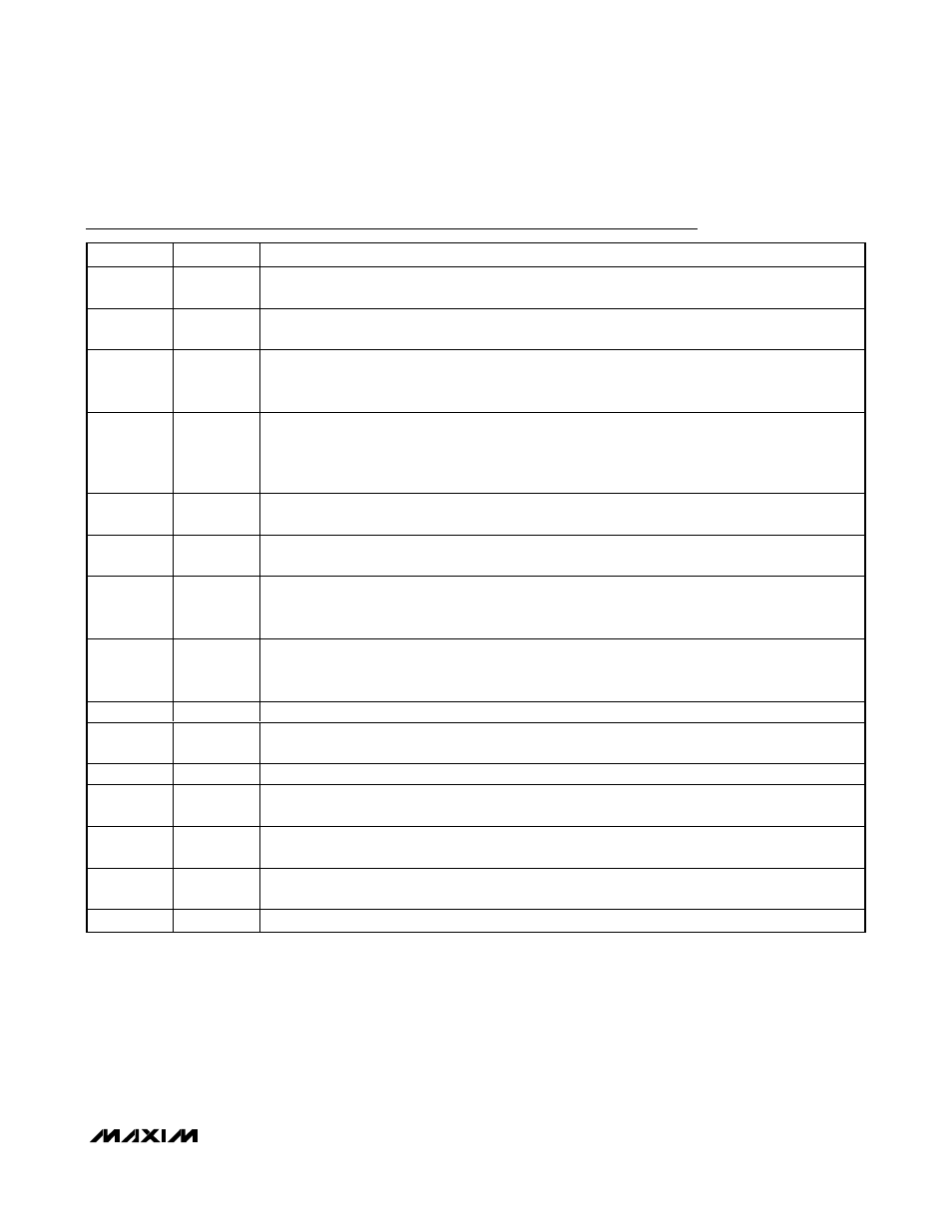
Pin Description
PIN
NAME
FUNCTION
1
SEL1
LDO Output-Voltage Select Input 1. SEL1 and SEL2 set the OUT1 and OUT2 voltages to one of nine
combinations (Table 1).
2
SEL2
LDO Output-Voltage Select Input 2. SEL1 and SEL2 set the OUT1 and OUT2 voltages to one of nine
combinations (Table 1).
3
EN2
OUT2 Enable Input. Drive EN2 low to enable OUT2. Drive EN2 high to disable OUT2. If the MAX8620Y
is placed into shutdown (PWR_ON = HF_PWR = low), OUT2 does not power regardless of the status
of EN2 (Table 2, Figure 4).
4
RESET
Open-Drain, Active-Low Reset Output. RESET asserts low when V
OUT1
drops below 87% (typ) of
regulation. RESET remains asserted for t
RP
after V
OUT1
rises above 87% (typ) of regulation. RESET
also asserts when OUT1 is disabled (Figure 4). RESET deasserts if OUT1 is enabled and V
OUT1
is
above 87% of regulation after t
RP
.
5
BP
Reference Bypass Capacitor Node. Bypass BP with a 0.01µF capacitor to GND. BP is high
impedance when the MAX8620Y is disabled (PWR_ON = HF_PWR = low).
6
HF_PWR
Hands-Free Enable Input. Drive HF_PWR high or apply a pulse to enable the MAX8620Y. Power is
enabled for 1.31s (typ) following a rising edge at HF_PWR (Table 2, Figure 4).
7
PWR_ON
Power-Enable Input. Drive PWR_ON high to enable the MAX8620Y (Table 2, Figure 4). Drive PWR_ON
low to enter shutdown mode. In shutdown, the LX node is high impedance and both LDOs are
disabled (depending on the state of HF_PWR).
8
FB
Step-Down Converter Output-Voltage Feedback Input. V
FB
regulates to 0.6V (typ). Connect FB to the
center of an external resistor-divider between LX and GND to set V
OUT3
between 0.6V and 3.3V (see
the Setting the Step-Down Output Voltage (OUT3) section).
9
GND
Ground. Connect GND to the exposed pad.
10
LX
Inductor Connection. LX is internally connected to the drain of the internal p-channel power MOSFET
and the drain of the n-channel synchronous rectifier. LX is high impedance when OUT3 is disabled.
11
IN2
Power Input 2. Connect IN2 to IN1 as close to the device as possible.
12
IN1
Power Input 1. Connect IN1 to IN2 as close to the device as possible. Bypass IN1 to GND with a 10µF
ceramic capacitor, as close to the device as possible.
13
OUT1
300mA LDO Output 1. Bypass OUT1 to GND with a 4.7µF ceramic capacitor for 300mA applications,
or a 2.2µF ceramic capacitor for 150mA applications. OUT1 is high impedance when disabled.
14
OUT2
300mA LDO Output 2. Bypass OUT2 to GND with a 4.7µF ceramic capacitor for 300mA applications,
or a 2.2µF ceramic capacitor for 150mA applications. OUT2 is high impedance when disabled.
EP
EP
Exposed Pad. Connect EP to GND.