U6820bm, Pin configuration, Pin description – Rainbow Electronics U6820BM User Manual
Page 2
2
U6820BM
4527A–BCD–03/02
Pin Configuration
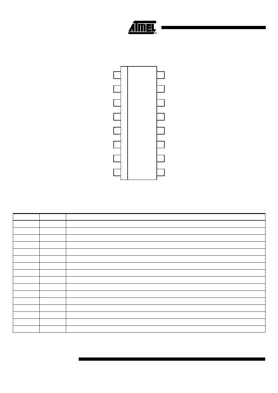
Figure 2. Pinning SO16
1
2
3
4
5
6
7
8
16
15
14
13
12
11
10
9
VS
GNDCC
GNDS
VCC
LS2
HS2
HS1
LS1
STATUS
DI
CLK
CS
LS3
HS3
HS4
LS4
Pin Description
Pin
Symbol
Function
1
HS1
Output high side 1
2
LS1
Output low side 1
3
VS
Supply voltage 6 V to 18 V
4
GNDCC
Digital ground
5
GNDS
Power ground
6
VCC
Supply voltage 5 V (external)
7
LS2
Output low side 2
8
HS2
Output high side 2
9
HS3
Output high side 3
10
LS3
Output low side 3
11
CS
Set supply status (chip select)
12
CLK
Clock line for 8-bit control shift register
13
DI
Data line for 8-bit control shift register
14
STATUS
Status output (H = fault, diagnostic “H” if all driver stages are switched off)
15
LS4
Output low side 4
16
HS4
Output high side 4