Applications information – Rainbow Electronics MAX7491 User Manual
Page 9

MAX7490/MAX7491
Dual Universal Switched-Capacitor Filters
_______________________________________________________________________________________
9
2nd-Order Filter Stage
The MAX7490/MAX7491 are dual biquad filters. The
biquad topology allows the use of standard filter tables
and equations to implement simultaneous lowpass,
bandpass, and notch or highpass filters. Topologies
such as Butterworth, Chebyshev, Bessel, elliptic, as
well as custom algorithms are possible.
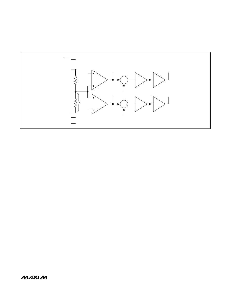
Internal Common Voltage
The COM pin sets the common-mode input voltage and
is internally biased to V
DD
/2 with a resistor-divider. The
resistors used are typically 250k
Ω for the MAX7490,
and typically 80k
Ω for the MAX7491. The common-
mode voltage is easily overdriven by an external volt-
age supply if desired. The COM pin should be
bypassed to the analog ground with at least a 0.1µF
capacitor.
Inverting Inputs
Locate resistors that are connected to INV_ as close as
possible to INV_ to reduce stray capacitance and noise
pickup. INV_ are inverting inputs to continuous-time op
amps, and behave like a virtual ground. There is no
sampling energy present on these inputs.
Outputs
Each switched-capacitor section, together with two to
four external resistors, can generate all standard 2nd-
order functions: bandpass, lowpass, highpass, and
notch (band-reject) functions. Three of these functions
are simultaneously available. The maximum signal
swing is limited by the power-supply voltages used.
The amplifiers’ outputs in the MAX7490/MAX7491 are
able to swing to within approximately 0.2V of either
supply.
Driving coaxial cable, large capacitive loads, or total
resistive loads less than 10k
Ω will degrade the total
harmonic distortion (THD) performance. Note that the
effective resistive load at the output must include both
the feedback resistors and any external load resistors.
Low-Power Shutdown Mode
The MAX7490/MAX7491 have a shutdown mode that is
activated by driving SHDN low. In shutdown mode, the
filter supply current reduces to <1µA (max), and the fil-
ter outputs become high impedance. The COM input
also becomes high impedance during shutdown. For
normal operation, drive SHDN high or connect to V
DD
.
__________Applications Information
Designing with the MAX7490/MAX7491 begins by
selecting the mode that best fits the desired circuit
requirements. Table 1 lists the available modes and
their relative advantages and disadvantages. Table 2
lists the different nomenclature used in the explanations
that follow.
Mode 1
Figure 2 shows the MAX7490/MAX7491s’ configuration
of Mode 1. This mode provides 2nd-order notch, low-
pass, and bandpass filter functions. The gain at all
three outputs is inversely proportional to the value of
R1. The center frequency, f
O
, is fixed at f
CLK
/100. High-
Q bandpass filters can be built without exceeding the
bandpass amplifier’s output swing (i.e., H
OBP
does not
Σ
∫
∫
NA/HPA (3)
SHDN
V
DD
(8)
GND (7)
CLK (9)
EXTCLK (10)
INVB (13)
COM (11)
R
R
INVA (4)
(6)
SA (5)
BPA (2)
LPA (1)
+
-
Σ
∫
∫
NB/HPB (14)
SB (12)
BPB (15)
LPB (16)
+
-
Figure 1. Block Diagram
