Rainbow Electronics MAX7491 User Manual
Page 15
MAX7490/MAX7491
Dual Universal Switched-Capacitor Filters
______________________________________________________________________________________
15
Input Signal Amplitude Range
The optimal input signal range is determined by
observing the voltage level at which the signal-to-noise
plus distortion (SINAD) ratio is maximized for a given
corner frequency. The Typical Operating Character-
istics show the THD + Noise response as the input sig-
nal’s peak-to-peak amplitude is varied. In most
systems, the input signal should be kept as large as
possible to maximize the signal-to-noise ratio (SNR).
Allow sufficient headroom to ensure no signal clipping
under expected operating conditions.
Anti-Aliasing and Post-DAC Filtering
When using the MAX7490/MAX7491 for anti-aliasing or
post-DAC filtering, synchronize the DAC (or ADC) and
the filter clocks. If the clocks are not synchronized,
beat frequencies may alias into the desired passband.
Aliasing
Aliasing is an inherent phenomenon of most switched-
capacitor filters. As with all sampled systems, frequen-
cy components of the input signal above one half the
sampling rate will be aliased. The MAX7490/MAX7491
sample at twice the clock frequency, yielding a 200:1
sampling to cutoff frequency ratio.
In particular, input signal components (f
IN
) near the
sampling rate generate a difference frequency
(f
SAMPLING
- f
IN
) that often falls within the passband of
the filter. Such aliased signals, when they appear at the
output, are indistinguishable from real input informa-
tion. For example, the aliased output signal generated
when a 99kHz waveform is applied to a filter sampling
at 100kHz, (f
CLK
= 50kHz) is 1kHz. This waveform is an
attenuated version of the output that would result from
a true 1kHz input. Since sampling is done at twice the
clock frequency, the Nyquist frequency is the same as
the clock frequency.
A simple passive RC lowpass input filter is usually suffi-
cient to remove input frequencies that can be aliased.
In many cases, the input signal itself may be band limit-
ed and require no special anti-alias filtering. Selecting
a passive filter cutoff frequency equal to f
C
/2 gives
12dB rejection at the Nyquist frequency.
Clock Feedthrough
Clock feedthrough is defined as the RMS value of the
clock frequency and its harmonics that are present at
the filter’s output pins, even without input signal. The
clock feedthrough can be greatly reduced by adding a
simple RC lowpass network at the final filter output.
Choose a cutoff frequency as low as possible to pro-
vide maximum noise attenuation. The attenuation and
phase shift of the external filter will limit the actual fre-
quency selected.
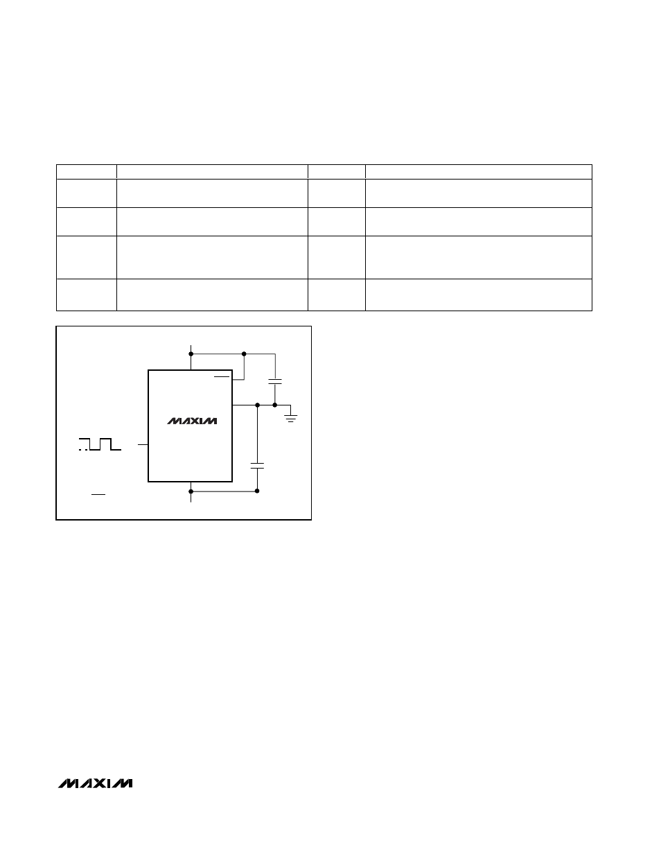
V
DD
V+
V-
CLK
GND
0.1
µF
CLOCK
*DRIVE SHDN TO V- FOR LOW-POWER
SHUTDOWN MODE.
SHDN
COM
0.1
µF
MAX7490
MAX7491
*
V+
V-
Figure 9. Dual-Supply Operation
MODE
VOSN/HP
VOSBP
VOSLP
1
V
OS1
[1 + (R2 / R3) + (R2 / R1)] - (V
OS3
)
(R2 / R3)
V
OS3
V
OSN/HP
- V
OS2
1b
V
OS1
[1 + (R2 / R3) + (R2 / R1)] - (V
OS3
)
(R2 / R3)
V
OS3
(V
OSN/HP
- V
OS2
)[1 + R5 / R6)]
2
V
OS1
[1 + (R2 / R3) + (R2 / R1) + (R2 / R4) -
(V
OS3
)(R2 / R3)][R4 / R2 + R4] +
(V
OS2
)[R2 / R2 + R4]
V
OS3
V
OSN/HP
- V
OS2
3
V
OS2
V
OS3
V
OS1
[1 + (R4 / R1) + (R4 / R2) + (R4 / R3)] - (V
OS2
)
(R4 / R2) - (V
OS3
)(R4 / R3)
Table 4. Output DC Offsets for a 2nd-Order Section