Detailed description, Pin description – Rainbow Electronics MAX7491 User Manual
Page 8
MAX7490/MAX7491
Dual Universal Switched-Capacitor Filters
8
_______________________________________________________________________________________
_______________Detailed Description
The MAX7490/MAX7491 are universal switched-capaci-
tor filters designed with a fixed internal f
CLK
/f
O
ratio of
100:1. Operating modes use external resistors connect-
ed in different arrangements to realize different filter
functions (highpass, lowpass, bandpass, notch) in all of
the classical filter topologies (Butterworth, Bessel, ellip-
tic, Chebyshev). Figure 1 shows a block diagram.
Clock Signal
External Clock
The MAX7490/MAX7491 switched-capacitor filters are
designed for use with external clocks that have a 50%
±5% duty cycle. When using an external clock, drive
the EXTCLK pin high or connect to V
DD
. Drive CLK with
CMOS logic levels (GND and V
DD
). Varying the rate of
the external clock adjusts the center frequency of the
filter:
f
O
= f
CLK
/100
Internal Clock
When using the internal oscillator, drive the EXTCLK pin
low or connect to GND and connect a capacitor (C
OSC
)
between CLK and GND. The value of the capacitor
(C
OSC
) determines the oscillator frequency as follows:
f
OSC
(kHz) = 135 x 10
3
/ C
OSC
(pF)
Since C
OSC
is in the low picofarads, minimize the stray
capacitance at CLK so that it does not affect the inter-
nal oscillator frequency. Varying the frequency of the
internal oscillator adjusts the filter’s center frequency by
a 100:1 clock-to-center frequency ratio. For example,
an internal oscillator frequency of 135kHz produces a
nominal center frequency of 1.35kHz.
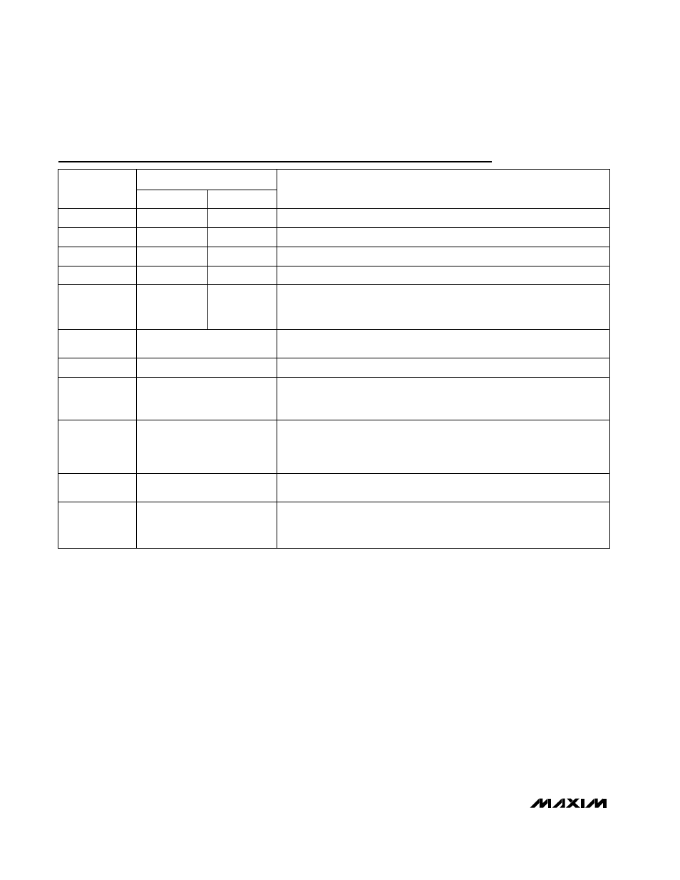
NAME
PIN
FILTER A
FILTER B
FUNCTION
LP_
1
16
2nd-Order Lowpass Filter Output
BP_
2
15
2nd-Order Bandpass Filter Output
N_/HP_
3
14
2nd-Order Notch/Highpass Filter Output
INV_
4
13
Inverting Input of Filter Summing Op Amp
S_
5
12
Summing Input. The connection of the summing input, along with the other
resistor connections, determine the circuit topology (mode) of each 2nd-
order section. S_ must never be left floating.
SHDN
6
Shutdown Input. Drive SHDN low to enable shutdown mode; drive high or
connect to V
DD
for normal operation.
GND
7
Ground Pin
V
DD
8
Positive Supply. V
DD
should be bypassed with a 0.1
µF capacitor to GND. A
low-noise supply is recommended. Input +5V for MAX7490 or +3V for
MAX7491.
CLK
9
Clock Input. Connect to an external capacitor (C
OSC
) between CLK and
ground to set the internal oscillator frequency. For external clock operation,
drive with a CMOS-level clock. The duty cycle of the external clock should be
between 45% and 55% for best performance.
EXTCLK
10
External/Internal Clock Select Input. Connect EXTCLK to V
DD
when driving
CLK externally. Connect to GND when using the internal oscillator.
COM
11
Common Pin. Biased internally at V
DD
/2. Bypass externally to GND with
0.1
µF capacitor. To override the internal biasing, drive with an external low-
impedance source.
Pin Description