Table 3. suggested external op amps – Rainbow Electronics MAX7491 User Manual
Page 14
MAX7490/MAX7491
Dual Universal Switched-Capacitor Filters
14
______________________________________________________________________________________
Mode 3A Design Equations
Note: When the passband gain error exceeds 1dB, the
use of capacitor C
C
between the lowpass output and
the inverting input will reduce the gain error. The value
can best be determined experimentally. Typically, it
should be about 5pF/dB (C
C-MAX
= 15pF).
Offset Voltage
Switched-capacitor integrators generally exhibit higher
input offsets than discrete RC integrators. The larger
offset is mainly due to the charge injection of the
CMOS switches into the integrating capacitors. The
internal op amp offset also adds to the overall offset
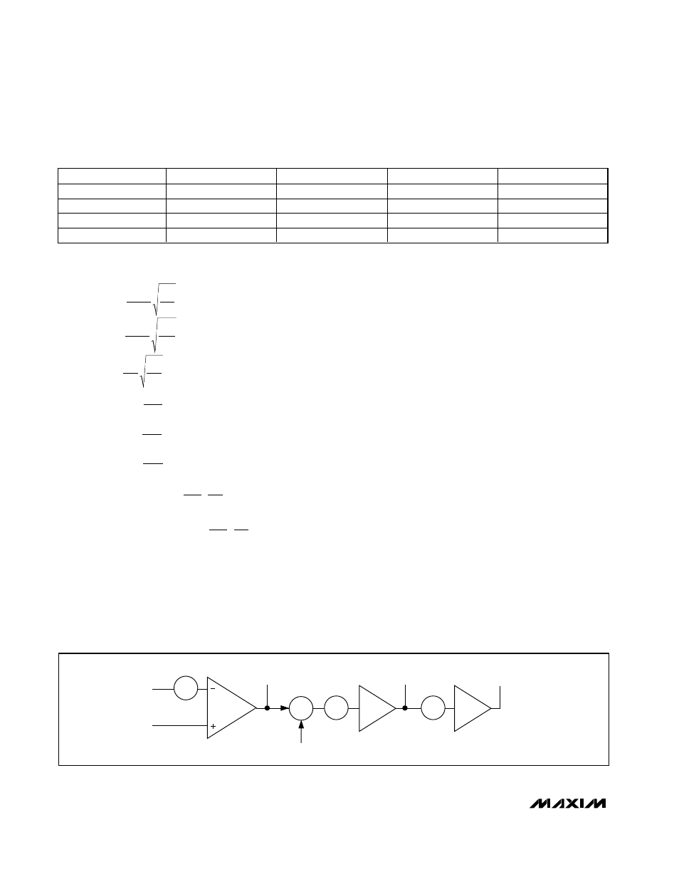
value. Figure 8 shows the input offsets from a single
2nd-order section. Table 4 lists the formula for the out-
put offset voltage for various modes and output pins.
Power Supplies
The MAX7490 operates from a single +5V supply, and
the MAX7491 operates from a single +3V supply.
Bypass V
DD
to GND with at least a 0.1µF capacitor.
V
DD
should be isolated from other digital or high-volt-
age analog supplies. If dual supplies are required,
connect the COM pin to the system ground and the
GND pin to the negative supply. Figure 9 shows an
example of dual-supply operation. Single-supply and
dual-supply performances are equivalent. For dual-
supply operation, drive CLK, SHDN, and EXTCLK from
GND (which is now V-) to V
DD
. If using the internal
oscillator in dual-supply mode, C
OSC
can be returned
to either GND or the actual ground voltage. Use the
MAX7490 for ±2.5V and use the MAX7491 for ±1.5V.
For most applications, a 0.1µF bypass capacitor from
COM to GND is sufficient. If the V
DD
supply has signifi-
cant 60Hz energy, increase this capacitor to 1µF or
greater to provide better power-supply rejection.
f
f
R
R
f
f
R
R
Q
R
R
R
R
H
R
R
H
R
R
H
R
R
H
f
Hz
R
R
R
R
H
at f
f
R
R
R
R
O
CLK
n
CLK
H
L
OHP
OLP
OBP
ON
G
L
ON
CLK
G
H
=
=
=
=
=
=
→
=
=
=
−
−
−
100
2
4
100
3
2
2
4
2
1
4
1
3
1
0
4
1
2
2
1
1
2
(
)
(
/ )
Figure 8. Block Diagram of a 2nd-Order Section Showing the Input Offsets
Σ
∫
∫
N/HP
S
INV
BP
LP
COM
V
OS1
V
OS2
V
OS3
+
-
PART
GBW (MHz)
SLEW RATE (V/
µs)
ISUPPLY/AMP (mA)
PIN-PACKAGE
MAX4281
2
0.7
0.5
5 SOT23
MAX4322
5
2.0
1.1
5 SOT23
MAX4130
10
4.0
1.15
5 SOT23
MAX4490
10
10.0
2.0
5 SOT23
Table 3. Suggested External Op Amps