Rainbow Electronics MAX7491 User Manual
Page 2
MAX7490/MAX7491
Dual Universal Switched-Capacitor Filters
2
_______________________________________________________________________________________
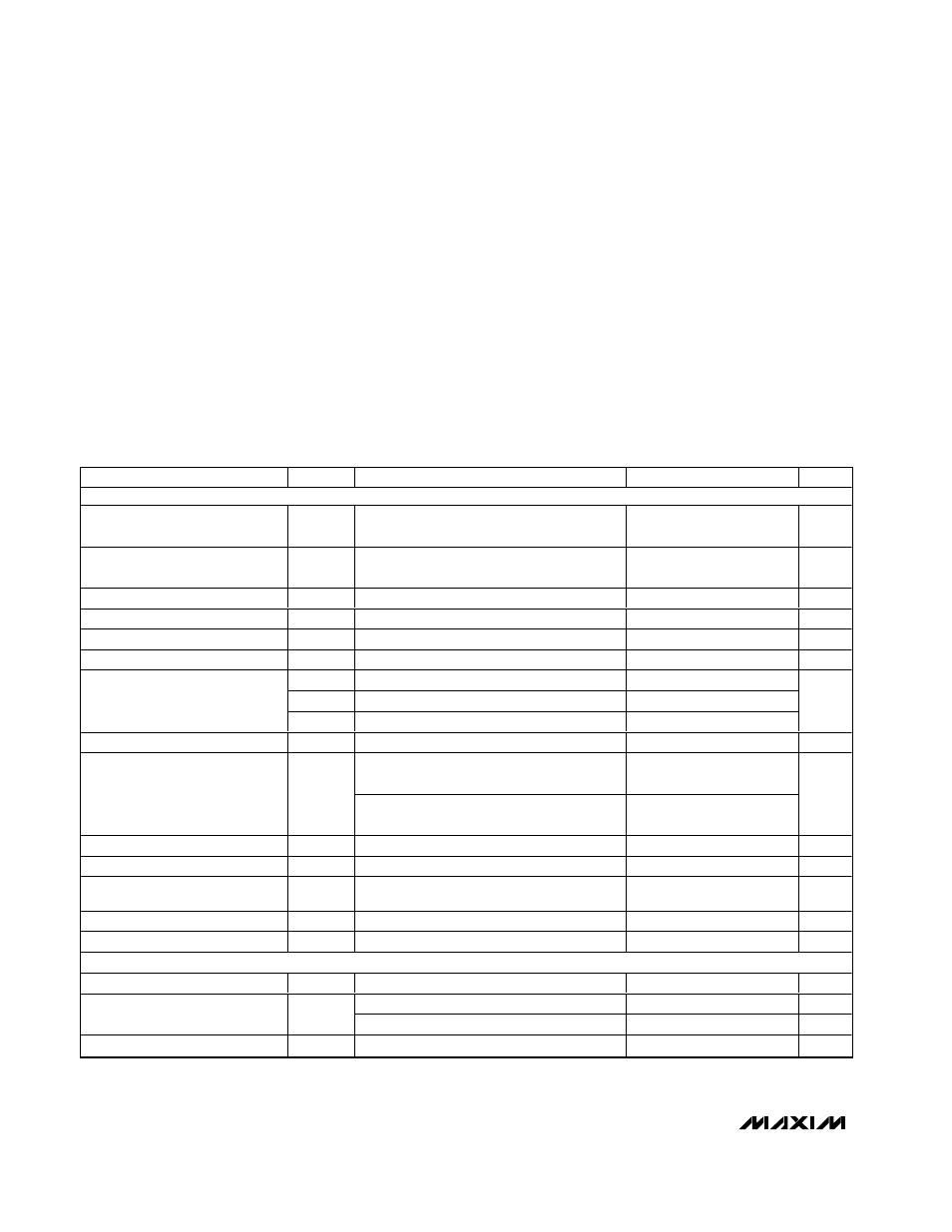
ABSOLUTE MAXIMUM RATINGS
ELECTRICAL CHARACTERISTICS—MAX7490
(V
DD
= EXTCLK = +5V, f
CLK
= 625kHz, T
A
= T
MIN
to T
MAX
, 10k
Ω || 50pF load to V
DD
/2 at LP_, BP_, and N_/HP_, SHDN = V
DD
, 0.1µF
from COM to GND, 50% duty-cycle clock input, COM = V
DD
/2. Typical values are at T
A
= +25°C, unless otherwise noted.) (Note 1)
Stresses beyond those listed under “Absolute Maximum Ratings” may cause permanent damage to the device. These are stress ratings only, and functional
operation of the device at these or any other conditions beyond those indicated in the operational sections of the specifications is not implied. Exposure to
absolute maximum rating conditions for extended periods may affect device reliability.
V
DD
to GND ..............................................................-0.3V to +6V
EXTCLK, SHDN to GND ...........................................-0.3V to +6V
INV_, LP_, BP_, N_/HP_, S_, COM,
CLK to GND............................................-0.3V to (V
DD
+ 0.3V)
Maximum Current into Any Pin ...........................................50mA
Continuous Power Dissipation (T
A
= +70°C)
16-Pin QSOP (derate 8.30mW/°C above +70°C).........667mW
Operating Temperature Range
MAX749_CEE ....................................................0°C to +70°C
MAX749_EEE ..................................................-40°C to +85°C
Die Temperature ..............................................................+150°C
Storage Temperature.........................................-65°C to +150°C
Lead Temperature (soldering, 10s) .................................+300°C
PARAMETER
SYMBOL
CONDITIONS
MIN
TYP
MAX
UNITS
FILTER
Center Frequency Range
f
O
Mode 1
0.001 to
40
kHz
Clock-to-Center Frequency
Accuracy
f
CLK
/f
O
Mode 1, R1 = R3 = 50k
Ω , R2 = 10kΩ,
Q = 5, deviation from 100:1
±0.2
±0.7
%
Q Accuracy
M od e 1, R1 = R3 = 50k
Ω, R2 = 10kΩ, Q = 5
±0.2
±2
%
f
O
Temperature Coefficient
±1
ppm/
°C
Q Temperature Coefficient
±5
ppm/
°C
DC Lowpass Gain Accuracy
Mode 1, R1 = R2 = 10k
Ω
±0.1
±0.5
%
V
OS1
DC offset of input inverter
±3
±12.5
V
OS2
DC offset of 1st integrator
±4
±15
DC Offset Voltage (Figure 8)
V
OS3
DC offset of 2nd integrator
±4
±30
mV
Crosstalk (Note 2)
f
IN
= 10kHz
-60
dB
Input: COM externally driven
V
DD
/2
- 0.5
V
DD
/2
V
DD
/2
+ 0.5
COM Voltage Range
V
COM
Output: COM internally driven
V
DD
/2
- 0.2
V
DD
/2
V
DD
/2
+ 0.2
V
Input Resistance at COM
R
COM
140
250
325
k
Ω
Clock Feedthrough
Up to 5th harmonic of f
CLK
200
µV
RMS
Noise (Note 3)
Mode 1, R1 = R2 = R3 =10k
Ω, LP output,
Q = 1
60
µV
RMS
Output Voltage Swing
0.2
V
D D
- 0.2
V
Input Leakage Current at COM
SHDN = GND, V
COM
= 0 to V
DD
±0.1
±10
µA
CLOCK
Maximum Clock Frequency
f
CLK
4
MHz
EXTCLK = GND, C
OSC
= 1000pF
95
135
175
kHz
Internal Oscillator Frequency
(Note 4)
f
OSC
EXTCLK = GND, C
OSC
= 100pF
1.35
MHz
Clock Input High
V
DD
- 0.5
V